Home > Press > Nanonics Imaging Ltd Receives 2015 Microscopy Today Innovation Award
 |
Abstract:
Nanonics Imaging Ltd Receives 2015 Microscopy Today Innovation Award
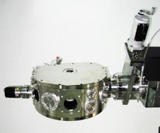
Nanonics is the proud recipient of the 2015 Microscopy Today Innovation Award for development of the CryoView MP system for low temperature, multiprobe scanning probe microscopy. These innovation awards are presented for the top 10 innovations in the field of microscopy by Microscopy and Analysis magazine and were presented at the 2015 Microscopy and Microanalysis conference in Portland, Oregon in August. This award follows the 2013 Microscopy Today award to Nanonics Imaging for its AFM-SEM-FIB microscope. These awards acknowledge outstanding advances in scientific research by Nanonics Imaging, including scanning probe microscopy, Nanonics’ area of expertise.
Nanonics Imaging Ltd Receives 2015 Microscopy Today Innovation Award
Jerusalem, Israel | Posted on September 8th, 2015The Nanonics Imaging CryoView MP was recognized for its innovation as a multi-probe scanning probe microscopy (SPM) platform designed to study mechanical, spectroscopic, optical, thermal, and electrical properties at low temperature. By employing up to four individual SPM probes that can be operated independently and simultaneously, the CryoView MP can perform a variety of characterization and transport measurements in situ in combination with light microscopy techniques such as Raman, fluorescence, and NSOM in a controlled environment from room temperature down to 10 K. Advanced forms of SPM are enabled for each individual probe including AFM, KPM, EFM, S-NSOM, NSOM, STM, AFM-Raman, and TERS.
Applications are possible over a range of temperatures such as: (a) electrical probe station combined with in situ simultaneous Raman characterization, (b) nanoscale optical and electrical transport measurements, where one probe serves as the excitation source and the second probe maps the transport process, (c) chemical lithography with one probe and high resolution imaging of the written features with a second probe, and (d) combined SPM measurements where one probe can perform an advanced SPM measurement while a high resolution AFM tip maps the same area.
A particular application of the CryoView MP is characterization of 2D materials such as graphene, MoS2, BN, NBSe2, metamaterials, and metasurfaces as well as other functional materials such as Si, carbon nanotubes, III-V semiconductors, and quantum dots. In order to fully examine the potential of these materials, multiple characterization methods need to be brought together in a single instrument like the CryoView MP to provide a complete understanding of their performance.
####
About Nanonics Imaging Ltd
Nanonics Imaging Ltd has developed a unique and highly differentiated product portfolio in the area of Scanning Probe Microscopy (SPM). Over the last two decades its products have stood at the forefront of technology providing answers for a wide range of nanotechnological applications unavailable with other measurement tools.
In this area of SPM, Nanonics Imaging is one of the most innovative companies in the world and this innovation together with unparalleled customer support and collaboration has been the basis of its growth. Today Nanonics has 45 employees in its Jerusalem headquarters and representatives throughout the world.
For more information, please click here
Contacts:
Dalia Yablon, Ph.D.
SurfaceChar LLC
www.surfacechar.com
Copyright © Nanonics Imaging Ltd
If you have a comment, please Contact us.Issuers of news releases, not 7th Wave, Inc. or Nanotechnology Now, are solely responsible for the accuracy of the content.
Bookmark:


| Related News Press |
News and information
![]() Quantum computer improves AI predictions April 17th, 2026
Quantum computer improves AI predictions April 17th, 2026
![]() Flexible sensor gains sensitivity under pressure April 17th, 2026
Flexible sensor gains sensitivity under pressure April 17th, 2026
![]() A reusable chip for particulate matter sensing April 17th, 2026
A reusable chip for particulate matter sensing April 17th, 2026
![]() Detecting vibrational quantum beating in the predissociation dynamics of SF6 using time-resolved photoelectron spectroscopy April 17th, 2026
Detecting vibrational quantum beating in the predissociation dynamics of SF6 using time-resolved photoelectron spectroscopy April 17th, 2026
Imaging
![]() Simple algorithm paired with standard imaging tool could predict failure in lithium metal batteries August 8th, 2025
Simple algorithm paired with standard imaging tool could predict failure in lithium metal batteries August 8th, 2025
Announcements
![]() A fundamentally new therapeutic approach to cystic fibrosis: Nanobody repairs cellular defect April 17th, 2026
A fundamentally new therapeutic approach to cystic fibrosis: Nanobody repairs cellular defect April 17th, 2026
![]() UC Irvine physicists discover method to reverse ‘quantum scrambling’ : The work addresses the problem of information loss in quantum computing system April 17th, 2026
UC Irvine physicists discover method to reverse ‘quantum scrambling’ : The work addresses the problem of information loss in quantum computing system April 17th, 2026
Tools
![]() Metasurfaces smooth light to boost magnetic sensing precision January 30th, 2026
Metasurfaces smooth light to boost magnetic sensing precision January 30th, 2026
![]() From sensors to smart systems: the rise of AI-driven photonic noses January 30th, 2026
From sensors to smart systems: the rise of AI-driven photonic noses January 30th, 2026
![]() Japan launches fully domestically produced quantum computer: Expo visitors to experience quantum computing firsthand August 8th, 2025
Japan launches fully domestically produced quantum computer: Expo visitors to experience quantum computing firsthand August 8th, 2025
Grants/Sponsored Research/Awards/Scholarships/Gifts/Contests/Honors/Records
![]() Quantum computer improves AI predictions April 17th, 2026
Quantum computer improves AI predictions April 17th, 2026
![]() Detecting vibrational quantum beating in the predissociation dynamics of SF6 using time-resolved photoelectron spectroscopy April 17th, 2026
Detecting vibrational quantum beating in the predissociation dynamics of SF6 using time-resolved photoelectron spectroscopy April 17th, 2026
![]() Metasurfaces smooth light to boost magnetic sensing precision January 30th, 2026
Metasurfaces smooth light to boost magnetic sensing precision January 30th, 2026
|
|
||
|
|
||
| The latest news from around the world, FREE | ||
|
|
||
|
|
||
| Premium Products | ||
|
|
||
|
Only the news you want to read!
Learn More |
||
|
|
||
|
Full-service, expert consulting
Learn More |
||
|
|
||