Home > Press > FEI Launches New DualBeam Plasma Focused Ion Beam for Electrical Fault Isolation & Failure Analysis: New Helios PFIB EFI is a fully-integrated deprocessing and fault isolation solution that reduces analysis time from days to just hours
 |
Abstract:
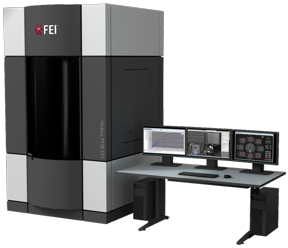
FEI (NASDAQ: FEIC) today launched a new DualBeam™ plasma focused ion beam (PFIB) for sample preparation, electrical fault isolation (EFI) and electrical failure analysis (EFA) on sub-20nm semiconductor devices. The Helios PFIB EFI is the only fully-integrated solution that improves time-to-results from days to just a few hours.
FEI Launches New DualBeam Plasma Focused Ion Beam for Electrical Fault Isolation & Failure Analysis: New Helios PFIB EFI is a fully-integrated deprocessing and fault isolation solution that reduces analysis time from days to just hours
Hillsboro, OR | Posted on June 4th, 2015“Semiconductor process development and yield enhancement engineers no longer need to suffer delays due to a multi-tool, multi-operator approach to electrical fault isolation and failure analysis,” states Rob Krueger, vice president and general manager of FEI’s semiconductor business. “The new Helios PFIB EFI is a fully-integrated, easy-to-use solution that cuts down the number of steps and sample transfers during the process. Eliminating these bottlenecks helps to reduce the process debug and device analysis cycle time by 50-80 percent and improve yields to near 100 percent, enabling chip makers to achieve significantly faster time-to-volume manufacturing.”
The Helios PFIB EFI is built upon the world’s most advanced DualBeam Plasma FIB platform with fully-integrated SEM and nanoprobing capabilities, delivering site-specific sample preparation with in-situ SEM end-pointing and low-beam energy SEM-based transistor characterization. It includes electron-beam absorbed current (EBAC) for interconnect-level electrical fault isolation and electron-beam induced current (EBIC) analysis for diffusion characterization. The system boosts deprocessing yields for 10nm devices by using FEI’s unique Dx delayering solution.
“Our proprietary Dx beam chemistry delivers high-yield, high-throughput sample prep at the sub-16nm and 14nm nodes, while low beam-energy SEM permits accurate in situ end-pointing, high-resolution imaging and precise electrical probe positioning,” continues Krueger. “Using the Helios PFIB EFI, our customers have successfully probed devices down to contact level for complete electrical analysis without degrading the transistor’s electrical properties.”
####
About FEI Company
FEI Company (Nasdaq: FEIC) designs, manufactures and supports a broad range of high-performance microscopy workflow solutions that provide images and answers at the micro-, nano- and picometer scales. Its innovation and leadership enable customers in industry and science to increase productivity and make breakthrough discoveries. Headquartered in Hillsboro, Ore., USA, FEI has over 2,600 employees and sales and service operations in more than 50 countries around the world. More information can be found at: www.fei.com.
FEI Safe Harbor Statement
This news release contains forward-looking statements that include statements regarding the performance capabilities and benefits of the Helios PFIB EFI and Dx delayering solution. Factors that could affect these forward-looking statements include but are not limited to our ability to manufacture, ship, deliver and install the tools, solutions or software as expected; failure of the product or technology to perform as expected; unexpected technology problems and challenges; changes to the technology; the inability of FEI, its suppliers or project partners to make the technological advances required for the technology to achieve anticipated results; and the inability of the customer to deploy the tools or develop and deploy the expected new applications. Please also refer to our Form 10-K, Forms 10-Q, Forms 8-K and other filings with the U.S. Securities and Exchange Commission for additional information on these factors and other factors that could cause actual results to differ materially from the forward-looking statements. FEI assumes no duty to update forward-looking statements.
For more information, please click here
Contacts:
Sandy Fewkes (media contact)
MindWrite Communications, Inc.
+1 408 224 4024
FEI Company
Jason Willey
(investors and analysts)
Investor Relations Director
+1 503 726 2533
Copyright © FEI Company
If you have a comment, please Contact us.Issuers of news releases, not 7th Wave, Inc. or Nanotechnology Now, are solely responsible for the accuracy of the content.
Bookmark:


| Related News Press |
News and information
![]() Quantum computer improves AI predictions April 17th, 2026
Quantum computer improves AI predictions April 17th, 2026
![]() Flexible sensor gains sensitivity under pressure April 17th, 2026
Flexible sensor gains sensitivity under pressure April 17th, 2026
![]() A reusable chip for particulate matter sensing April 17th, 2026
A reusable chip for particulate matter sensing April 17th, 2026
![]() Detecting vibrational quantum beating in the predissociation dynamics of SF6 using time-resolved photoelectron spectroscopy April 17th, 2026
Detecting vibrational quantum beating in the predissociation dynamics of SF6 using time-resolved photoelectron spectroscopy April 17th, 2026
Imaging
![]() Simple algorithm paired with standard imaging tool could predict failure in lithium metal batteries August 8th, 2025
Simple algorithm paired with standard imaging tool could predict failure in lithium metal batteries August 8th, 2025
Chip Technology
![]() A reusable chip for particulate matter sensing April 17th, 2026
A reusable chip for particulate matter sensing April 17th, 2026
![]() Metasurfaces smooth light to boost magnetic sensing precision January 30th, 2026
Metasurfaces smooth light to boost magnetic sensing precision January 30th, 2026
Announcements
![]() A fundamentally new therapeutic approach to cystic fibrosis: Nanobody repairs cellular defect April 17th, 2026
A fundamentally new therapeutic approach to cystic fibrosis: Nanobody repairs cellular defect April 17th, 2026
![]() UC Irvine physicists discover method to reverse ‘quantum scrambling’ : The work addresses the problem of information loss in quantum computing system April 17th, 2026
UC Irvine physicists discover method to reverse ‘quantum scrambling’ : The work addresses the problem of information loss in quantum computing system April 17th, 2026
Tools
![]() Metasurfaces smooth light to boost magnetic sensing precision January 30th, 2026
Metasurfaces smooth light to boost magnetic sensing precision January 30th, 2026
![]() From sensors to smart systems: the rise of AI-driven photonic noses January 30th, 2026
From sensors to smart systems: the rise of AI-driven photonic noses January 30th, 2026
![]() Japan launches fully domestically produced quantum computer: Expo visitors to experience quantum computing firsthand August 8th, 2025
Japan launches fully domestically produced quantum computer: Expo visitors to experience quantum computing firsthand August 8th, 2025
|
|
||
|
|
||
| The latest news from around the world, FREE | ||
|
|
||
|
|
||
| Premium Products | ||
|
|
||
|
Only the news you want to read!
Learn More |
||
|
|
||
|
Full-service, expert consulting
Learn More |
||
|
|
||