Home > Press > Caltech scientists develop cool process to make better graphene
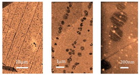 |
| These are images of early-stage growth of graphene on copper. The lines of hexagons are graphene nuclei, with increasing magnification from left to right, where the scale bars from left to right correspond to 10 μm, 1 μm, and 200 nm, respectively. The hexagons grow together into a seamless sheet of graphene. CREDIT: Courtesy of D. Boyd and N. Yeh labs/Caltech |
Abstract:
A new technique invented at Caltech to produce graphene--a material made up of an atom-thick layer of carbon--at room temperature could help pave the way for commercially feasible graphene-based solar cells and light-emitting diodes, large-panel displays, and flexible electronics.
Caltech scientists develop cool process to make better graphene
Pasadena, CA | Posted on March 18th, 2015"With this new technique, we can grow large sheets of electronic-grade graphene in much less time and at much lower temperatures," says Caltech staff scientist David Boyd, who developed the method.
Boyd is the first author of a new study, published in the March 18 issue of the journal Nature Communications, detailing the new manufacturing process and the novel properties of the graphene it produces.
Graphene could revolutionize a variety of engineering and scientific fields due to its unique properties, which include a tensile strength 200 times stronger than steel and an electrical mobility that is two to three orders of magnitude better than silicon. The electrical mobility of a material is a measure of how easily electrons can travel across its surface.
However, achieving these properties on an industrially relevant scale has proven to be complicated. Existing techniques require temperatures that are much too hot--1,800 degrees Fahrenheit, or 1,000 degrees Celsius--for incorporating graphene fabrication with current electronic manufacturing. Additionally, high-temperature growth of graphene tends to induce large, uncontrollably distributed strain--deformation--in the material, which severely compromises its intrinsic properties.
"Previously, people were only able to grow a few square millimeters of high-mobility graphene at a time, and it required very high temperatures, long periods of time, and many steps," says Caltech physics professor Nai-Chang Yeh, the Fletcher Jones Foundation Co-Director of the Kavli Nanoscience Institute and the corresponding author of the new study. "Our new method can consistently produce high-mobility and nearly strain-free graphene in a single step in just a few minutes without high temperature. We have created sample sizes of a few square centimeters, and since we think that our method is scalable, we believe that we can grow sheets that are up to several square inches or larger, paving the way to realistic large-scale applications."
The new manufacturing process might not have been discovered at all if not for a fortunate turn of events. In 2012, Boyd, then working in the lab of the late David Goodwin, at that time a Caltech professor of mechanical engineering and applied physics, was trying to reproduce a graphene-manufacturing process he had read about in a scientific journal. In this process, heated copper is used to catalyze graphene growth. "I was playing around with it on my lunch hour," says Boyd, who now works with Yeh's research group. "But the recipe wasn't working. It seemed like a very simple process. I even had better equipment than what was used in the original experiment, so it should have been easier for me."
During one of his attempts to reproduce the experiment, the phone rang. While Boyd took the call, he unintentionally let a copper foil heat for longer than usual before exposing it to methane vapor, which provides the carbon atoms needed for graphene growth.
When later Boyd examined the copper plate using Raman spectroscopy, a technique used for detecting and identifying graphene, he saw evidence that a graphene layer had indeed formed. "It was an 'A-ha!' moment," Boyd says. "I realized then that the trick to growth is to have a very clean surface, one without the copper oxide."
As Boyd recalls, he then remembered that Robert Millikan, a Nobel Prize-winning physicist and the head of Caltech from 1921 to 1945, also had to contend with removing copper oxide when he performed his famous 1916 experiment to measure Planck's constant, which is important for calculating the amount of energy a single particle of light, or photon, Boyd wondered if he, like Millikan, could devise a method for cleaning his copper while it was under vacuum conditions.
The solution Boyd hit upon was to use a system first developed in the 1960s to generate a hydrogen plasma--that is, hydrogen gas that has been electrified to separate the electrons from the protons--to remove the copper oxide at much lower temperatures. His initial experiments revealed not only that the technique worked to remove the copper oxide, but that it simultaneously produced graphene as well.
At first, Boyd could not figure out why the technique was so successful. He later discovered that two leaky valves were letting in trace amounts of methane into the experiment chamber. "The valves were letting in just the right amount of methane for graphene to grow," he says.
The ability to produce graphene without the need for active heating not only reduces manufacturing costs, but also results in a better product because fewer defects--introduced as a result of thermal expansion and contraction processes--are generated. This in turn eliminates the need for multiple postproduction steps. "Typically, it takes about ten hours and nine to ten different steps to make a batch of high-mobility graphene using high-temperature growth methods," Yeh says. "Our process involves one step, and it takes five minutes."
Work by Yeh's group and international collaborators later revealed that graphene made using the new technique is of higher quality than graphene made using conventional methods: It is stronger because it contains fewer defects that could weaken its mechanical strength, and it has the highest electrical mobility yet measured for synthetic graphene.
The team thinks one reason their technique is so efficient is that a chemical reaction between the hydrogen plasma and air molecules in the chamber's atmosphere generates cyano radicals--carbon-nitrogen molecules that have been stripped of their electrons. Like tiny superscrubbers, these charged molecules effectively scour the copper of surface imperfections providing a pristine surface on which to grow graphene.
The scientists also discovered that their graphene grows in a special way. Graphene produced using conventional thermal processes grows from a random patchwork of depositions. But graphene growth with the plasma technique is more orderly. The graphene deposits form lines that then grow into a seamless sheet, which contributes to its mechanical and electrical integrity.
A scaled-up version of their plasma technique could open the door for new kinds of electronics manufacturing, Yeh says. For example, graphene sheets with low concentrations of defects could be used to protect materials against degradation from exposure to the environment. Another possibility would be to grow large sheets of graphene that can be used as a transparent conducting electrode for solar cells and display panels. "In the future, you could have graphene-based cell-phone displays that generate their own power," Yeh says.
Another possibility, she says, is to introduce intentionally imperfections into graphene's lattice structure to create specific mechanical and electronic attributes. "If you can strain graphene by design at the nanoscale, you can artificially engineer its properties. But for this to work, you need to start with a perfectly smooth, strain-free sheet of graphene," Yeh says. "You can't do this if you have a sheet of graphene that has uncontrollable defects in different places."
###
Along with Yeh and Boyd, additional authors on the paper, "Single-Step Deposition of High-Mobility Graphene at Reduced Temperatures," include Caltech graduate students Wei Hsiang Lin, Chen Chih Hsu and Chien-Chang Chen; Caltech staff scientist Marcus Teague; Yuan-Yen Lo, Tsung-Chih Cheng, and Chih-I Wu of National Taiwan University; and Wen-Yuan Chan, Wei-Bing Su, and Chia-Seng Chang of the Institute of Physics, Academia Sinica.
####
For more information, please click here
Contacts:
Deborah Williams-Hedges
626-395-3227
Copyright © California Institute of Technology
If you have a comment, please Contact us.Issuers of news releases, not 7th Wave, Inc. or Nanotechnology Now, are solely responsible for the accuracy of the content.
Bookmark:


| Related News Press |
News and information
![]() Quantum computer improves AI predictions April 17th, 2026
Quantum computer improves AI predictions April 17th, 2026
![]() Flexible sensor gains sensitivity under pressure April 17th, 2026
Flexible sensor gains sensitivity under pressure April 17th, 2026
![]() A reusable chip for particulate matter sensing April 17th, 2026
A reusable chip for particulate matter sensing April 17th, 2026
![]() Detecting vibrational quantum beating in the predissociation dynamics of SF6 using time-resolved photoelectron spectroscopy April 17th, 2026
Detecting vibrational quantum beating in the predissociation dynamics of SF6 using time-resolved photoelectron spectroscopy April 17th, 2026
Flexible Electronics
![]() Flexible sensor gains sensitivity under pressure April 17th, 2026
Flexible sensor gains sensitivity under pressure April 17th, 2026
![]() Flexible electronics integrated with paper-thin structure for use in space January 17th, 2025
Flexible electronics integrated with paper-thin structure for use in space January 17th, 2025
Display technology/LEDs/SS Lighting/OLEDs
![]() Spinel-type sulfide semiconductors to operate the next-generation LEDs and solar cells For solar-cell absorbers and green-LED source October 3rd, 2025
Spinel-type sulfide semiconductors to operate the next-generation LEDs and solar cells For solar-cell absorbers and green-LED source October 3rd, 2025
Graphene/ Graphite
![]() Electrifying results shed light on graphene foam as a potential material for lab grown cartilage June 6th, 2025
Electrifying results shed light on graphene foam as a potential material for lab grown cartilage June 6th, 2025
Discoveries
![]() Quantum computer improves AI predictions April 17th, 2026
Quantum computer improves AI predictions April 17th, 2026
![]() Flexible sensor gains sensitivity under pressure April 17th, 2026
Flexible sensor gains sensitivity under pressure April 17th, 2026
![]() A reusable chip for particulate matter sensing April 17th, 2026
A reusable chip for particulate matter sensing April 17th, 2026
![]() Detecting vibrational quantum beating in the predissociation dynamics of SF6 using time-resolved photoelectron spectroscopy April 17th, 2026
Detecting vibrational quantum beating in the predissociation dynamics of SF6 using time-resolved photoelectron spectroscopy April 17th, 2026
Announcements
![]() A fundamentally new therapeutic approach to cystic fibrosis: Nanobody repairs cellular defect April 17th, 2026
A fundamentally new therapeutic approach to cystic fibrosis: Nanobody repairs cellular defect April 17th, 2026
![]() UC Irvine physicists discover method to reverse �quantum scrambling� : The work addresses the problem of information loss in quantum computing system April 17th, 2026
UC Irvine physicists discover method to reverse �quantum scrambling� : The work addresses the problem of information loss in quantum computing system April 17th, 2026
Interviews/Book Reviews/Essays/Reports/Podcasts/Journals/White papers/Posters
![]() A fundamentally new therapeutic approach to cystic fibrosis: Nanobody repairs cellular defect April 17th, 2026
A fundamentally new therapeutic approach to cystic fibrosis: Nanobody repairs cellular defect April 17th, 2026
![]() UC Irvine physicists discover method to reverse �quantum scrambling� : The work addresses the problem of information loss in quantum computing system April 17th, 2026
UC Irvine physicists discover method to reverse �quantum scrambling� : The work addresses the problem of information loss in quantum computing system April 17th, 2026
Energy
![]() Sensors innovations for smart lithium-based batteries: advancements, opportunities, and potential challenges August 8th, 2025
Sensors innovations for smart lithium-based batteries: advancements, opportunities, and potential challenges August 8th, 2025
![]() Simple algorithm paired with standard imaging tool could predict failure in lithium metal batteries August 8th, 2025
Simple algorithm paired with standard imaging tool could predict failure in lithium metal batteries August 8th, 2025
Research partnerships
![]() Lab to industry: InSe wafer-scale breakthrough for future electronics August 8th, 2025
Lab to industry: InSe wafer-scale breakthrough for future electronics August 8th, 2025
![]() HKU physicists uncover hidden order in the quantum world through deconfined quantum critical points April 25th, 2025
HKU physicists uncover hidden order in the quantum world through deconfined quantum critical points April 25th, 2025
Solar/Photovoltaic
![]() Spinel-type sulfide semiconductors to operate the next-generation LEDs and solar cells For solar-cell absorbers and green-LED source October 3rd, 2025
Spinel-type sulfide semiconductors to operate the next-generation LEDs and solar cells For solar-cell absorbers and green-LED source October 3rd, 2025
![]() KAIST researchers introduce new and improved, next-generation perovskite solar cell November 8th, 2024
KAIST researchers introduce new and improved, next-generation perovskite solar cell November 8th, 2024
![]() Groundbreaking precision in single-molecule optoelectronics August 16th, 2024
Groundbreaking precision in single-molecule optoelectronics August 16th, 2024
![]() Development of zinc oxide nanopagoda array photoelectrode: photoelectrochemical water-splitting hydrogen production January 12th, 2024
Development of zinc oxide nanopagoda array photoelectrode: photoelectrochemical water-splitting hydrogen production January 12th, 2024
|
|
||
|
|
||
| The latest news from around the world, FREE | ||
|
|
||
|
|
||
| Premium Products | ||
|
|
||
|
Only the news you want to read!
Learn More |
||
|
|
||
|
Full-service, expert consulting
Learn More |
||
|
|
||