Home > Press > High-precision positioning of wafers in inspection systems
 |
Abstract:
The current standard wafer has a diameter of 8". The industry is moving towards manufacturing larger wafers. Technologies for production processes such as stealth dicing, lithography, doping, implanting, planarization makes precise positioning of the bigger substrates a must. Thin film technology places great demands on the substrates and their structures. The piezosystem jena GmbH now offers a positioning system for the inspection of the new larger wafers.
High-precision positioning of wafers in inspection systems
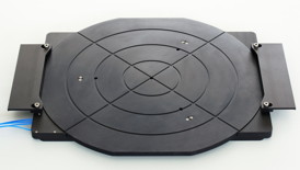
Jena, Germany | Posted on July 8th, 2014The new system offered by piezosystem jena system is designed to position wafers with a diameter up to 12" using precise hold and repeat positioning with the same precise precision. The system can be used as an automated inline controller or as a stand-alone positioner. The highly precise positioning system allows steady processes in production and process control. The new system will also shorten cycle times in quality control. Piezosystem jena's new system offers positioning in microseconds with steps of a few microns with repeatability in nanometers. Your crucial data will be obtained quickly with excellent performance and value.
Requirements:
�measuring range < 300 �m
�small, repeatable steps
�movement free of displacement
�short rise time
�controlled positioning
Applications:
�semi conductor and solar producing
�lithography
�display production
�surface structuring
�surface inspection
�measurement chips
�measurement of conductor tracks
�measurement systems
�quality control
�bonding-technology
####
For more information, please click here
Contacts:
Theresa Kuntze
Copyright © Piezosystem Jena GmbH
If you have a comment, please Contact us.Issuers of news releases, not 7th Wave, Inc. or Nanotechnology Now, are solely responsible for the accuracy of the content.
Bookmark:


| Related News Press |
News and information
![]() Quantum computer improves AI predictions April 17th, 2026
Quantum computer improves AI predictions April 17th, 2026
![]() Flexible sensor gains sensitivity under pressure April 17th, 2026
Flexible sensor gains sensitivity under pressure April 17th, 2026
![]() A reusable chip for particulate matter sensing April 17th, 2026
A reusable chip for particulate matter sensing April 17th, 2026
![]() Detecting vibrational quantum beating in the predissociation dynamics of SF6 using time-resolved photoelectron spectroscopy April 17th, 2026
Detecting vibrational quantum beating in the predissociation dynamics of SF6 using time-resolved photoelectron spectroscopy April 17th, 2026
Chip Technology
![]() A reusable chip for particulate matter sensing April 17th, 2026
A reusable chip for particulate matter sensing April 17th, 2026
![]() Metasurfaces smooth light to boost magnetic sensing precision January 30th, 2026
Metasurfaces smooth light to boost magnetic sensing precision January 30th, 2026
Announcements
![]() A fundamentally new therapeutic approach to cystic fibrosis: Nanobody repairs cellular defect April 17th, 2026
A fundamentally new therapeutic approach to cystic fibrosis: Nanobody repairs cellular defect April 17th, 2026
![]() UC Irvine physicists discover method to reverse �quantum scrambling� : The work addresses the problem of information loss in quantum computing system April 17th, 2026
UC Irvine physicists discover method to reverse �quantum scrambling� : The work addresses the problem of information loss in quantum computing system April 17th, 2026
Tools
![]() Metasurfaces smooth light to boost magnetic sensing precision January 30th, 2026
Metasurfaces smooth light to boost magnetic sensing precision January 30th, 2026
![]() From sensors to smart systems: the rise of AI-driven photonic noses January 30th, 2026
From sensors to smart systems: the rise of AI-driven photonic noses January 30th, 2026
![]() Japan launches fully domestically produced quantum computer: Expo visitors to experience quantum computing firsthand August 8th, 2025
Japan launches fully domestically produced quantum computer: Expo visitors to experience quantum computing firsthand August 8th, 2025
|
|
||
|
|
||
| The latest news from around the world, FREE | ||
|
|
||
|
|
||
| Premium Products | ||
|
|
||
|
Only the news you want to read!
Learn More |
||
|
|
||
|
Full-service, expert consulting
Learn More |
||
|
|
||