Home > Press > Tiny compound semiconductor transistor could challenge silicon’s dominance --MIT researchers develop the smallest indium gallium arsenide transistor ever built
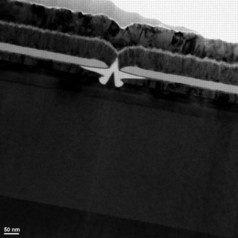 |
| A cross-section transmission electron micrograph of the fabricated transistor. The central inverted V is the gate. The two molybdenum contacts on either side are the source and drain of the transistor. The channel is the indium gallium arsenide light color layer under the source, drain and gate. Image courtesy of the researchers |
Abstract:
Silicon's crown is under threat: The semiconductor's days as the king of microchips for computers and smart devices could be numbered, thanks to the development of the smallest transistor ever to be built from a rival material, indium gallium arsenide.
Tiny compound semiconductor transistor could challenge silicon’s dominance --MIT researchers develop the smallest indium gallium arsenide transistor ever built
Cambridge, MA | Posted on December 10th, 2012The compound transistor, built by a team in MIT's Microsystems Technology Laboratories, performs well despite being just 22 nanometers (billionths of a meter) in length. This makes it a promising candidate to eventually replace silicon in computing devices, says co-developer Jesús del Alamo, the Donner Professor of Science in MIT's Department of Electrical Engineering and Computer Science (EECS), who built the transistor with EECS graduate student Jianqian Lin and Dimitri Antoniadis, the Ray and Maria Stata Professor of Electrical Engineering.
To keep pace with our demand for ever-faster and smarter computing devices, the size of transistors is continually shrinking, allowing increasing numbers of them to be squeezed onto microchips. "The more transistors you can pack on a chip, the more powerful the chip is going to be, and the more functions the chip is going to perform," del Alamo says.
But as silicon transistors are reduced to the nanometer scale, the amount of current that can be produced by the devices is also shrinking, limiting their speed of operation. This has led to fears that Moore's Law — the prediction by Intel founder Gordon Moore that the number of transistors on microchips will double every two years — could be about to come to an end, del Alamo says.
To keep Moore's Law alive, researchers have for some time been investigating alternatives to silicon, which could potentially produce a larger current even when operating at these smaller scales. One such material is the compound indium gallium arsenide, which is already used in fiber-optic communication and radar technologies, and is known to have extremely good electrical properties, del Alamo says. But despite recent advances in treating the material to allow it to be formed into a transistor in a similar way to silicon, nobody has yet been able to produce devices small enough to be packed in ever-greater numbers into tomorrow's microchips.
Now del Alamo, Antoniadis and Lin have shown it is possible to build a nanometer-sized metal-oxide semiconductor field-effect transistor (MOSFET) — the type most commonly used in logic applications such as microprocessors — using the material. "We have shown that you can make extremely small indium gallium arsenide MOSFETs with excellent logic characteristics, which promises to take Moore's Law beyond the reach of silicon," del Alamo says.
Transistors consist of three electrodes: the gate, the source and the drain, with the gate controlling the flow of electrons between the other two. Since space in these tiny transistors is so tight, the three electrodes must be placed in extremely close proximity to each other, a level of precision that would be impossible for even sophisticated tools to achieve. Instead, the team allows the gate to "self-align" itself between the other two electrodes.
The researchers first grow a thin layer of the material using molecular beam epitaxy, a process widely used in the semiconductor industry in which evaporated atoms of indium, gallium and arsenic react with each other within a vacuum to form a single-crystal compound. The team then deposits a layer of molybdenum as the source and drain contact metal. They then "draw" an extremely fine pattern onto this substrate using a focused beam of electrons — another well-established fabrication technique known as electron beam lithography.
Unwanted areas of material are then etched away and the gate oxide is deposited onto the tiny gap. Finally, evaporated molybdenum is fired at the surface, where it forms the gate, tightly squeezed between the two other electrodes, del Alamo says. "Through a combination of etching and deposition we can get the gate nestled [between the electrodes] with tiny gaps around it," he says.
Although many of the techniques applied by the team are already used in silicon fabrication, they have only rarely been used to make compound semiconductor transistors. This is partly because in applications such as fiber-optic communication, space is less of an issue. "But when you are talking about integrating billions of tiny transistors onto a chip, then we need to completely reformulate the fabrication technology of compound semiconductor transistors to look much more like that of silicon transistors," del Alamo says.
The team presents its work this week at the International Electron Devices Meeting in San Francisco.
Their next step will be to work on further improving the electrical performance — and hence the speed — of the transistor by eliminating unwanted resistance within the device. Once they have achieved this, they will attempt to further shrink the device, with the ultimate aim of reducing the size of their transistor to below 10 nanometers in gate length.
The research was funded by DARPA and the Semiconductor Research Corporation.
Written by Helen Knight, MIT News Office
####
For more information, please click here
Contacts:
Caroline McCall
MIT News Office
T: 617-253-1682
Copyright © Massachusetts Institute of Technology
If you have a comment, please Contact us.Issuers of news releases, not 7th Wave, Inc. or Nanotechnology Now, are solely responsible for the accuracy of the content.
Bookmark:


| Related News Press |
News and information
![]() Quantum computer improves AI predictions April 17th, 2026
Quantum computer improves AI predictions April 17th, 2026
![]() Flexible sensor gains sensitivity under pressure April 17th, 2026
Flexible sensor gains sensitivity under pressure April 17th, 2026
![]() A reusable chip for particulate matter sensing April 17th, 2026
A reusable chip for particulate matter sensing April 17th, 2026
![]() Detecting vibrational quantum beating in the predissociation dynamics of SF6 using time-resolved photoelectron spectroscopy April 17th, 2026
Detecting vibrational quantum beating in the predissociation dynamics of SF6 using time-resolved photoelectron spectroscopy April 17th, 2026
Govt.-Legislation/Regulation/Funding/Policy
![]() Quantum computer improves AI predictions April 17th, 2026
Quantum computer improves AI predictions April 17th, 2026
![]() Metasurfaces smooth light to boost magnetic sensing precision January 30th, 2026
Metasurfaces smooth light to boost magnetic sensing precision January 30th, 2026
![]() New imaging approach transforms study of bacterial biofilms August 8th, 2025
New imaging approach transforms study of bacterial biofilms August 8th, 2025
Chip Technology
![]() A reusable chip for particulate matter sensing April 17th, 2026
A reusable chip for particulate matter sensing April 17th, 2026
![]() Metasurfaces smooth light to boost magnetic sensing precision January 30th, 2026
Metasurfaces smooth light to boost magnetic sensing precision January 30th, 2026
Discoveries
![]() Quantum computer improves AI predictions April 17th, 2026
Quantum computer improves AI predictions April 17th, 2026
![]() Flexible sensor gains sensitivity under pressure April 17th, 2026
Flexible sensor gains sensitivity under pressure April 17th, 2026
![]() A reusable chip for particulate matter sensing April 17th, 2026
A reusable chip for particulate matter sensing April 17th, 2026
![]() Detecting vibrational quantum beating in the predissociation dynamics of SF6 using time-resolved photoelectron spectroscopy April 17th, 2026
Detecting vibrational quantum beating in the predissociation dynamics of SF6 using time-resolved photoelectron spectroscopy April 17th, 2026
Announcements
![]() A fundamentally new therapeutic approach to cystic fibrosis: Nanobody repairs cellular defect April 17th, 2026
A fundamentally new therapeutic approach to cystic fibrosis: Nanobody repairs cellular defect April 17th, 2026
![]() UC Irvine physicists discover method to reverse ‘quantum scrambling’ : The work addresses the problem of information loss in quantum computing system April 17th, 2026
UC Irvine physicists discover method to reverse ‘quantum scrambling’ : The work addresses the problem of information loss in quantum computing system April 17th, 2026
Military
![]() Quantum engineers ‘squeeze’ laser frequency combs to make more sensitive gas sensors January 17th, 2025
Quantum engineers ‘squeeze’ laser frequency combs to make more sensitive gas sensors January 17th, 2025
![]() Chainmail-like material could be the future of armor: First 2D mechanically interlocked polymer exhibits exceptional flexibility and strength January 17th, 2025
Chainmail-like material could be the future of armor: First 2D mechanically interlocked polymer exhibits exceptional flexibility and strength January 17th, 2025
![]() Single atoms show their true color July 5th, 2024
Single atoms show their true color July 5th, 2024
![]() NRL charters Navy’s quantum inertial navigation path to reduce drift April 5th, 2024
NRL charters Navy’s quantum inertial navigation path to reduce drift April 5th, 2024
Alliances/Trade associations/Partnerships/Distributorships
![]() Chicago Quantum Exchange welcomes six new partners highlighting quantum technology solutions, from Chicago and beyond September 23rd, 2022
Chicago Quantum Exchange welcomes six new partners highlighting quantum technology solutions, from Chicago and beyond September 23rd, 2022
![]() University of Illinois Chicago joins Brookhaven Lab's Quantum Center June 10th, 2022
University of Illinois Chicago joins Brookhaven Lab's Quantum Center June 10th, 2022
|
|
||
|
|
||
| The latest news from around the world, FREE | ||
|
|
||
|
|
||
| Premium Products | ||
|
|
||
|
Only the news you want to read!
Learn More |
||
|
|
||
|
Full-service, expert consulting
Learn More |
||
|
|
||