Home > Press > Tighter 'stitching' means better graphene, say scientists
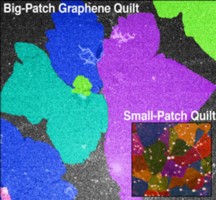 |
| Muller lab False-color microscopy images show examples of graphene grown slowly, resulting in large patches with poor stitching, and graphene grown more quickly, resulting in smaller patches with tighter stitching and better performance. |
Abstract:
Similar to how tighter stiches make for a better quality quilt, the "stitching" between individual crystals of graphene affects how well these carbon monolayers conduct electricity and retain their strength, Cornell researchers report.
Tighter 'stitching' means better graphene, say scientists
Ithaca, NY | Posted on June 4th, 2012The quality of this "stitching" -- the boundaries at which graphene crystals grow together and form sheets -- is just as important as the size of the crystals themselves, which scientists had previously thought held the key to making better graphene.
The researchers, led by Jiwoong Park, assistant professor of chemistry and chemical biology and a member of the Kavli Institute at Cornell for Nanoscale Science, used advanced measurement and imaging techniques to make these claims, detailed online in the journal Science June 1.
Graphene is a single layer of carbon atoms, and materials scientists are engaged in a sort of arms race to manipulate and enhance its amazing properties -- tensile strength, high electrical conductance, and potential applications in photonics, photovoltaics and electronics. Cartoons depict graphene like a perfect atomic chicken wire stretching ad infinitum.
In reality, graphene is polycrystalline; it is grown via a process called chemical vapor deposition, in which small crystals, or grains, at random orientations grow by themselves and eventually join together in carbon-carbon bonds.
In earlier work published in Nature last January, the Cornell group had used electron microscopy to liken these graphene sheets to patchwork quilts -- each "patch" represented by the orientation of the graphene grains (and false colored to make them pretty).
They, along with other scientists, wondered how graphene's electrical properties would hold up based on its polycrystalline nature. Conventional wisdom and some prior indirect measurements had led scientists to surmise that growing graphene with larger crystals -- fewer patches -- might improve its properties.
The new work questions that dogma. The group compared how graphene performed based on different rates of growth via chemical vapor deposition; some they grew more slowly, and others, very quickly. They found that the more reactive, quick-growth graphene, with more patches, in certain ways performed better electronically than the slower growth graphene with larger patches.
As it turned out, faster growth led to tighter stitching between grains, which improved the graphene's performance, as opposed to larger grains that were more loosely held together.
"What's important here is that we need to promote the growth environment so that the grains stitch together well," Park said. "What we are showing is that grain boundaries were a main concern, but it could be that it doesn't matter. We are finding that it's probably OK."
Equal in importance to these observations were the complex techniques they used to make the measurements -- no easy task. A four-step electron beam lithography process, developed by Adam Tsen, an applied physics graduate student and the paper's first author, allowed the researchers to place electrodes on graphene, directly on top of a 10 nanometer-thick membrane substrate to measure electrical properties of single grain boundaries.
"Our technique sets a tone for how we can measure atomically thin materials in the future," Park added.
Collaborators led by David A. Muller, professor of applied and engineering physics and co-director of the Kavli Institute at Cornell for Nanoscale Science, used advanced transmission electron microscopy techniques to help Park's group image their graphene to show the differences in the grain sizes.
The work was supported by the Air Force Office of Scientific Research, and the National Science Foundation through the Cornell Center for Materials Research. Fabrication was performed at the Cornell NanoScale Science and Technology Facility.
####
For more information, please click here
Contacts:
Media Contact:
John Carberry
(607) 255-5353
Cornell Chronicle:
Anne Ju
(607) 255-9735
Copyright © Cornell University
If you have a comment, please Contact us.Issuers of news releases, not 7th Wave, Inc. or Nanotechnology Now, are solely responsible for the accuracy of the content.
Bookmark:


| Related News Press |
News and information
![]() Decoding hydrogen‑bond network of electrolyte for cryogenic durable aqueous zinc‑ion batteries January 30th, 2026
Decoding hydrogen‑bond network of electrolyte for cryogenic durable aqueous zinc‑ion batteries January 30th, 2026
![]() COF scaffold membrane with gate‑lane nanostructure for efficient Li+/Mg2+ separation January 30th, 2026
COF scaffold membrane with gate‑lane nanostructure for efficient Li+/Mg2+ separation January 30th, 2026
![]() MXene nanomaterials enter a new dimension Multilayer nanomaterial: MXene flakes created at Drexel University show new promise as 1D scrolls January 30th, 2026
MXene nanomaterials enter a new dimension Multilayer nanomaterial: MXene flakes created at Drexel University show new promise as 1D scrolls January 30th, 2026
Imaging
![]() ICFO researchers overcome long-standing bottleneck in single photon detection with twisted 2D materials August 8th, 2025
ICFO researchers overcome long-standing bottleneck in single photon detection with twisted 2D materials August 8th, 2025
![]() Simple algorithm paired with standard imaging tool could predict failure in lithium metal batteries August 8th, 2025
Simple algorithm paired with standard imaging tool could predict failure in lithium metal batteries August 8th, 2025
Graphene/ Graphite
![]() Electrifying results shed light on graphene foam as a potential material for lab grown cartilage June 6th, 2025
Electrifying results shed light on graphene foam as a potential material for lab grown cartilage June 6th, 2025
![]() Breakthrough in proton barrier films using pore-free graphene oxide: Kumamoto University researchers achieve new milestone in advanced coating technologies September 13th, 2024
Breakthrough in proton barrier films using pore-free graphene oxide: Kumamoto University researchers achieve new milestone in advanced coating technologies September 13th, 2024
Govt.-Legislation/Regulation/Funding/Policy
![]() Metasurfaces smooth light to boost magnetic sensing precision January 30th, 2026
Metasurfaces smooth light to boost magnetic sensing precision January 30th, 2026
![]() New imaging approach transforms study of bacterial biofilms August 8th, 2025
New imaging approach transforms study of bacterial biofilms August 8th, 2025
![]() Electrifying results shed light on graphene foam as a potential material for lab grown cartilage June 6th, 2025
Electrifying results shed light on graphene foam as a potential material for lab grown cartilage June 6th, 2025
Chip Technology
![]() Metasurfaces smooth light to boost magnetic sensing precision January 30th, 2026
Metasurfaces smooth light to boost magnetic sensing precision January 30th, 2026
![]() Beyond silicon: Electronics at the scale of a single molecule January 30th, 2026
Beyond silicon: Electronics at the scale of a single molecule January 30th, 2026
![]() Lab to industry: InSe wafer-scale breakthrough for future electronics August 8th, 2025
Lab to industry: InSe wafer-scale breakthrough for future electronics August 8th, 2025
Discoveries
![]() From sensors to smart systems: the rise of AI-driven photonic noses January 30th, 2026
From sensors to smart systems: the rise of AI-driven photonic noses January 30th, 2026
![]() Decoding hydrogen‑bond network of electrolyte for cryogenic durable aqueous zinc‑ion batteries January 30th, 2026
Decoding hydrogen‑bond network of electrolyte for cryogenic durable aqueous zinc‑ion batteries January 30th, 2026
![]() COF scaffold membrane with gate‑lane nanostructure for efficient Li+/Mg2+ separation January 30th, 2026
COF scaffold membrane with gate‑lane nanostructure for efficient Li+/Mg2+ separation January 30th, 2026
Materials/Metamaterials/Magnetoresistance
![]() First real-time observation of two-dimensional melting process: Researchers at Mainz University unveil new insights into magnetic vortex structures August 8th, 2025
First real-time observation of two-dimensional melting process: Researchers at Mainz University unveil new insights into magnetic vortex structures August 8th, 2025
![]() Researchers unveil a groundbreaking clay-based solution to capture carbon dioxide and combat climate change June 6th, 2025
Researchers unveil a groundbreaking clay-based solution to capture carbon dioxide and combat climate change June 6th, 2025
![]() A 1960s idea inspires NBI researchers to study hitherto inaccessible quantum states June 6th, 2025
A 1960s idea inspires NBI researchers to study hitherto inaccessible quantum states June 6th, 2025
![]() Institute for Nanoscience hosts annual proposal planning meeting May 16th, 2025
Institute for Nanoscience hosts annual proposal planning meeting May 16th, 2025
Announcements
![]() Decoding hydrogen‑bond network of electrolyte for cryogenic durable aqueous zinc‑ion batteries January 30th, 2026
Decoding hydrogen‑bond network of electrolyte for cryogenic durable aqueous zinc‑ion batteries January 30th, 2026
![]() COF scaffold membrane with gate‑lane nanostructure for efficient Li+/Mg2+ separation January 30th, 2026
COF scaffold membrane with gate‑lane nanostructure for efficient Li+/Mg2+ separation January 30th, 2026
Tools
![]() Metasurfaces smooth light to boost magnetic sensing precision January 30th, 2026
Metasurfaces smooth light to boost magnetic sensing precision January 30th, 2026
![]() From sensors to smart systems: the rise of AI-driven photonic noses January 30th, 2026
From sensors to smart systems: the rise of AI-driven photonic noses January 30th, 2026
![]() Japan launches fully domestically produced quantum computer: Expo visitors to experience quantum computing firsthand August 8th, 2025
Japan launches fully domestically produced quantum computer: Expo visitors to experience quantum computing firsthand August 8th, 2025
Military
![]() Quantum engineers �squeeze� laser frequency combs to make more sensitive gas sensors January 17th, 2025
Quantum engineers �squeeze� laser frequency combs to make more sensitive gas sensors January 17th, 2025
![]() Chainmail-like material could be the future of armor: First 2D mechanically interlocked polymer exhibits exceptional flexibility and strength January 17th, 2025
Chainmail-like material could be the future of armor: First 2D mechanically interlocked polymer exhibits exceptional flexibility and strength January 17th, 2025
![]() Single atoms show their true color July 5th, 2024
Single atoms show their true color July 5th, 2024
![]() NRL charters Navy�s quantum inertial navigation path to reduce drift April 5th, 2024
NRL charters Navy�s quantum inertial navigation path to reduce drift April 5th, 2024
Printing/Lithography/Inkjet/Inks/Bio-printing/Dyes
![]() Presenting: Ultrasound-based printing of 3D materials�potentially inside the body December 8th, 2023
Presenting: Ultrasound-based printing of 3D materials�potentially inside the body December 8th, 2023
![]() Simple ballpoint pen can write custom LEDs August 11th, 2023
Simple ballpoint pen can write custom LEDs August 11th, 2023
![]() Disposable electronics on a simple sheet of paper October 7th, 2022
Disposable electronics on a simple sheet of paper October 7th, 2022
|
|
||
|
|
||
| The latest news from around the world, FREE | ||
|
|
||
|
|
||
| Premium Products | ||
|
|
||
|
Only the news you want to read!
Learn More |
||
|
|
||
|
Full-service, expert consulting
Learn More |
||
|
|
||