Home > Press > JEOL Introduces Ultra-high Resolution Analytical Field Emission SEM: Highest performance FE-SEM optimized for sub-nm resolution imaging of any type of sample
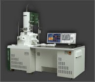 |
| JEOL JSM-7800F Ultra-High Resolution Analytical FE SEM |
Abstract:
JEOL's new series of field emission scanning electron microscopes is now complete with the introduction of the sub-nanometer imaging resolution JSM-7800F. The JSM-7800F represents a significant leap forward in Field Emission SEM technology, with unmatched resolution and stability for nanotechnology imaging and analysis.
JEOL Introduces Ultra-high Resolution Analytical Field Emission SEM: Highest performance FE-SEM optimized for sub-nm resolution imaging of any type of sample
Peabody, MA | Posted on May 31st, 2012JEOL's highest performance FE-SEM makes it possible to:
- observe the finest structural morphology of nanomaterials at 1,000,000X magnification with sub-1nm resolution
- perform low kV imaging and analysis of highly magnetic samples.
- collect large area EBSD maps at low magnifications without distortion
- image thin, electron transparent samples with sub 0.8 nm resolution using an optional retractable STEM detector
"JEOL now offers a full line of analytical, high performance electron microscopes to fit every technical performance requirement and budget," said Vern Robertson, SEM Technical Sales Manager at JEOL USA.
Optimized for extreme imaging and analysis
The JSM-7800F uniquely combines an in-lens field emission gun with an aperture angle control lens (ACL), optimizing large probe currents (up to 200 nA) for operation at the smallest probe diameter. The new super hybrid lens design and versatile in-column detectors with filtering capabilities allow observation of any specimen, especially at ultra-low accelerating voltages down to 10V. The SEM excels at low accelerating voltage X-ray spectroscopy and cathodoluminescence, combining large beam currents with a small interaction volume and dramatically increasing analytical resolution to the sub 100nm scale. Beam deceleration in GB Mode decreases charging on nonconductive samples and reduces lens aberration effects for extreme high resolution imaging.
Ultimate versatility
The JSM-7800F is suitable for a wide variety of applications, from cryo-microscopy to electron beam lithography, and can be configured for low vacuum operation. It accommodates multiple analytical attachments, including EDS, WDS, STEM, BSE, CL, EBIC, and an IR camera and stage navigation camera. The SEM comes with a choice of three stage sizes and three specimen exchange airlock sizes. It can also be equipped with tensile, heating, and cooling stages for in situ experiments.
www.jeolusa.com/PRODUCTS/ElectronOptics/ScanningElectronMicroscopesSEM/FESEM/JSM7800F/tabid/869/Default.aspx
####
About JEOL USA, Inc.
JEOL is a world leader in electron optical equipment and instrumentation for high-end scientific and industrial research and development. Core product groups include electron microscopes (SEMs and TEMs), instruments for the semiconductor industry (electron beam lithography and a series of defect review and inspection tools), and analytical instruments including mass spectrometers, NMRs and ESRs.
JEOL USA, Inc., a wholly owned subsidiary of JEOL, Ltd., Japan, was incorporated in the United States in 1962. The company has 13 regional service centers that offer unlimited emergency service and support in the U.S.
For more information, please click here
Contacts:
JEOL USA, Inc.
11 Dearborn Road
Peabody, MA 01960
978-535-5900
Copyright © JEOL USA, Inc.
If you have a comment, please Contact us.Issuers of news releases, not 7th Wave, Inc. or Nanotechnology Now, are solely responsible for the accuracy of the content.
Bookmark:


| Related News Press |
News and information
![]() Quantum computer improves AI predictions April 17th, 2026
Quantum computer improves AI predictions April 17th, 2026
![]() Flexible sensor gains sensitivity under pressure April 17th, 2026
Flexible sensor gains sensitivity under pressure April 17th, 2026
![]() A reusable chip for particulate matter sensing April 17th, 2026
A reusable chip for particulate matter sensing April 17th, 2026
![]() Detecting vibrational quantum beating in the predissociation dynamics of SF6 using time-resolved photoelectron spectroscopy April 17th, 2026
Detecting vibrational quantum beating in the predissociation dynamics of SF6 using time-resolved photoelectron spectroscopy April 17th, 2026
Imaging
![]() Simple algorithm paired with standard imaging tool could predict failure in lithium metal batteries August 8th, 2025
Simple algorithm paired with standard imaging tool could predict failure in lithium metal batteries August 8th, 2025
Announcements
![]() A fundamentally new therapeutic approach to cystic fibrosis: Nanobody repairs cellular defect April 17th, 2026
A fundamentally new therapeutic approach to cystic fibrosis: Nanobody repairs cellular defect April 17th, 2026
![]() UC Irvine physicists discover method to reverse �quantum scrambling� : The work addresses the problem of information loss in quantum computing system April 17th, 2026
UC Irvine physicists discover method to reverse �quantum scrambling� : The work addresses the problem of information loss in quantum computing system April 17th, 2026
Tools
![]() Metasurfaces smooth light to boost magnetic sensing precision January 30th, 2026
Metasurfaces smooth light to boost magnetic sensing precision January 30th, 2026
![]() From sensors to smart systems: the rise of AI-driven photonic noses January 30th, 2026
From sensors to smart systems: the rise of AI-driven photonic noses January 30th, 2026
![]() Japan launches fully domestically produced quantum computer: Expo visitors to experience quantum computing firsthand August 8th, 2025
Japan launches fully domestically produced quantum computer: Expo visitors to experience quantum computing firsthand August 8th, 2025
|
|
||
|
|
||
| The latest news from around the world, FREE | ||
|
|
||
|
|
||
| Premium Products | ||
|
|
||
|
Only the news you want to read!
Learn More |
||
|
|
||
|
Full-service, expert consulting
Learn More |
||
|
|
||