Home > Press > JEOL Introduces New Versatile FE-SEM Series for Sub-Nanometer Imaging and Analysis of Nanostructures and Magnetic Samples
 |
Abstract:
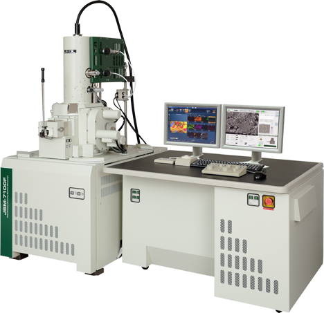
JEOL launches a new series of Field Emission Scanning Electron Microscopes (FE-SEM) that offer expanded imaging and analysis capabilities customizable to performance requirements. The JEOL JSM-7100F series offers sub-1 nm imaging capabilities and analytical characterization at the sub-100nm scale, accomplished through the combination of large beam currents with a small probe size at any accelerating voltage.
JEOL Introduces New Versatile FE-SEM Series for Sub-Nanometer Imaging and Analysis of Nanostructures and Magnetic Samples
Peabody, MA | Posted on April 17th, 2012Designed for the budget-conscious lab, the JSM-7100F model is a highly versatile, easy-to-use analytical field emission SEM that offers a new level of expanded performance. Through the unique 'in-lens field emission gun', the SEM delivers ≥ 200 nA of beam current to the sample. An aperture angle control lens (ACL) automatically optimizes both small probe current spot size for high resolution imaging and spot shape for high beam current, high resolution microanalysis, while a beam deceleration mode curtails charging on nonconductive specimens such as ceramics, semiconductors and polymers.
For advanced high resolution capabilities, the JSM-7100FT model features a newly redesigned hybrid lens and through-the lens detectors with energy filter. The superior electron optics design of this SEM column enables high resolution imaging of nanostructures and specimen surface details for any material type, including magnetic samples. With the integration of in-the-lens acceleration and deceleration of the electron beam, low kV aberrations are reduced, yielding higher resolution at the lowest accelerating voltages. Additionally, JEOL's proven beam deceleration mode (GB Mode) decreases charging while imaging non-conductive specimens, improves spot size at low kV, and enhances surface topography.
This new series of Field Emission SEMs offers increased versatility for multiple analytical techniques and imaging and analysis of non-conductive samples. Each microscope model features a turbo molecular pump (TMP) and a rapid specimen exchange airlock to assure a clean vacuum environment is always maintained.
Optional Low Vacuum Operation
The optional LV function (up to 300 Pa) offers additional versatility to both JSM-7100F and JSM-7100FT. The LV function is fully controlled through the microscope user interface and allows all LV orifices to be retracted without breaking vacuum for unrestricted low magnification imaging and maximum beam current (200 nA) in high vacuum. The LV system is equipped with a solid-state BSE detector.
Adaptable for Multiple Analytical Techniques
The JSM-7100F series is equipped with a large specimen chamber that accommodates a wide variety of detectors and accessories simultaneously and without compromising the performance of one another, including: multiple EDS, WDS, STEM, BSE, CL and IR camera. The system can also be equipped with a variety of sub stages including tensile, heating and cooling stages for in situ experimentation.
Enhanced Productivity
JEOL is renowned for its easy to use SEM operating software, graphical user interface, and productivity-enhancing functions. Stored images retain operating conditions and stage coordinates serving effectively as individual recipe functions, which is ideal in the multi-user environment. All image archiving, searching, measurement, report generation, filtering, and montaging can be conducted from the image database.
####
About JEOL USA, Inc.
JEOL is a world leader in electron optical equipment and instrumentation for high-end scientific and industrial research and development. Core product groups include electron microscopes (SEMs and TEMs), instruments for the semiconductor industry (electron beam lithography and a series of defect review and inspection tools), and analytical instruments including mass spectrometers, NMRs and ESRs.
JEOL USA, Inc., a wholly owned subsidiary of JEOL, Ltd., Japan, was incorporated in the United States in 1962. The company has 13 regional service centers that offer unlimited emergency service and support in the U.S.
For more information, please click here
Contacts:
Pamela Mansfield
Marketing Communications
JEOL USA
978.536.2309
Copyright © JEOL USA, Inc.
If you have a comment, please Contact us.Issuers of news releases, not 7th Wave, Inc. or Nanotechnology Now, are solely responsible for the accuracy of the content.
Bookmark:


| Related News Press |
News and information
![]() Quantum computer improves AI predictions April 17th, 2026
Quantum computer improves AI predictions April 17th, 2026
![]() Flexible sensor gains sensitivity under pressure April 17th, 2026
Flexible sensor gains sensitivity under pressure April 17th, 2026
![]() A reusable chip for particulate matter sensing April 17th, 2026
A reusable chip for particulate matter sensing April 17th, 2026
![]() Detecting vibrational quantum beating in the predissociation dynamics of SF6 using time-resolved photoelectron spectroscopy April 17th, 2026
Detecting vibrational quantum beating in the predissociation dynamics of SF6 using time-resolved photoelectron spectroscopy April 17th, 2026
Imaging
![]() Simple algorithm paired with standard imaging tool could predict failure in lithium metal batteries August 8th, 2025
Simple algorithm paired with standard imaging tool could predict failure in lithium metal batteries August 8th, 2025
Announcements
![]() A fundamentally new therapeutic approach to cystic fibrosis: Nanobody repairs cellular defect April 17th, 2026
A fundamentally new therapeutic approach to cystic fibrosis: Nanobody repairs cellular defect April 17th, 2026
![]() UC Irvine physicists discover method to reverse �quantum scrambling� : The work addresses the problem of information loss in quantum computing system April 17th, 2026
UC Irvine physicists discover method to reverse �quantum scrambling� : The work addresses the problem of information loss in quantum computing system April 17th, 2026
Tools
![]() Metasurfaces smooth light to boost magnetic sensing precision January 30th, 2026
Metasurfaces smooth light to boost magnetic sensing precision January 30th, 2026
![]() From sensors to smart systems: the rise of AI-driven photonic noses January 30th, 2026
From sensors to smart systems: the rise of AI-driven photonic noses January 30th, 2026
![]() Japan launches fully domestically produced quantum computer: Expo visitors to experience quantum computing firsthand August 8th, 2025
Japan launches fully domestically produced quantum computer: Expo visitors to experience quantum computing firsthand August 8th, 2025
|
|
||
|
|
||
| The latest news from around the world, FREE | ||
|
|
||
|
|
||
| Premium Products | ||
|
|
||
|
Only the news you want to read!
Learn More |
||
|
|
||
|
Full-service, expert consulting
Learn More |
||
|
|
||