Home > Press > New JEOL Through-the-Lens System for Ultrahigh Resolution SEM
 |
Abstract:
JEOL Scanning Electron Microscope Offers Versatile Through-the-Lens System for Ultrahigh Resolution
New JEOL Through-the-Lens System for Ultrahigh Resolution SEM
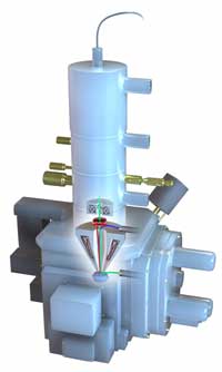
Peabody, MA | Posted on August 26th, 2010JEOL has introduced a unique Scanning Electron Microscope with optics that enable ultrahigh resolution imaging at low kV and high spatial resolution microanalysis. The Through-the-Lens System (TTLS) combines new objective lens and detector technologies with the proven JEOL in-lens Field Emission Gun. The TTLS is designed to enable imaging of a wide variety of samples, including magnetic materials. The model JSM-7001FTTLS LV also features low vacuum operation and a large specimen exchange airlock.
In the TTL System, in-lens detectors with energy filtering provide both topography (SE) and Z contrast (BSE) images. Short working distance, low currents, and low kV sensitivity ensure high resolution BSE images. Gentle Beam technology reduces charging and improves resolution, signal-to-noise, and beam brightness, especially at low beam voltages (down to 100V). The TTLS operates at low magnification (10X) with no distortion of the image or the EBSD pattern, allowing collection of large area EBSD maps of large grain materials.
The flexibility of this SEM is displayed in its ability to run in low vacuum (LV) mode for imaging nonconductive samples at high kV and beam currents for a variety of analytical applications that include analysis with EDS, WDS, EBSD, and CL. An optional STEM detector allows imaging of thin samples with sub 0.8nm resolution.
To learn more about the JEOL JSM-7001FTTLS LV SEM, please visit www.jeolusa.com or contact your local sales representative.
####
About JEOL
JEOL is a world leader in electron optical equipment and instrumentation for high-end scientific and industrial research and development. Core product groups include electron microscopes (SEMs and TEMs), instruments for the semiconductor industry (electron beam lithography and a series of defect review and inspection tools), and analytical instruments including mass spectrometers, NMRs and ESRs.
JEOL USA, Inc., is a wholly owned subsidiary of JEOL, Ltd., Japan, was incorporated in the United States in 1962. The company has 13 regional service centers that offer unlimited emergency service and support in the U.S.
For more information, please click here
Contacts:
Press Contact:
Patricia Corkum
Marketing Manager
JEOL USA
978-536-2273
Pamela Mansfield
JEOL USA
11 Dearborn Road
Peabody, MA 01960
978-536-2309
Copyright © JEOL
If you have a comment, please Contact us.Issuers of news releases, not 7th Wave, Inc. or Nanotechnology Now, are solely responsible for the accuracy of the content.
Bookmark:


| Related News Press |
News and information
![]() Quantum computer improves AI predictions April 17th, 2026
Quantum computer improves AI predictions April 17th, 2026
![]() Flexible sensor gains sensitivity under pressure April 17th, 2026
Flexible sensor gains sensitivity under pressure April 17th, 2026
![]() A reusable chip for particulate matter sensing April 17th, 2026
A reusable chip for particulate matter sensing April 17th, 2026
![]() Detecting vibrational quantum beating in the predissociation dynamics of SF6 using time-resolved photoelectron spectroscopy April 17th, 2026
Detecting vibrational quantum beating in the predissociation dynamics of SF6 using time-resolved photoelectron spectroscopy April 17th, 2026
Announcements
![]() A fundamentally new therapeutic approach to cystic fibrosis: Nanobody repairs cellular defect April 17th, 2026
A fundamentally new therapeutic approach to cystic fibrosis: Nanobody repairs cellular defect April 17th, 2026
![]() UC Irvine physicists discover method to reverse �quantum scrambling� : The work addresses the problem of information loss in quantum computing system April 17th, 2026
UC Irvine physicists discover method to reverse �quantum scrambling� : The work addresses the problem of information loss in quantum computing system April 17th, 2026
Tools
![]() Metasurfaces smooth light to boost magnetic sensing precision January 30th, 2026
Metasurfaces smooth light to boost magnetic sensing precision January 30th, 2026
![]() From sensors to smart systems: the rise of AI-driven photonic noses January 30th, 2026
From sensors to smart systems: the rise of AI-driven photonic noses January 30th, 2026
![]() Japan launches fully domestically produced quantum computer: Expo visitors to experience quantum computing firsthand August 8th, 2025
Japan launches fully domestically produced quantum computer: Expo visitors to experience quantum computing firsthand August 8th, 2025
|
|
||
|
|
||
| The latest news from around the world, FREE | ||
|
|
||
|
|
||
| Premium Products | ||
|
|
||
|
Only the news you want to read!
Learn More |
||
|
|
||
|
Full-service, expert consulting
Learn More |
||
|
|
||