Home > Press > For Nanowires, Nothing Sparkles Quite Like Diamond
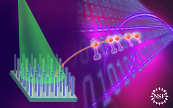 |
| A new diamond nanowire matrix yields a stream of single photons emitted when excited by green light |
Abstract:
Diamond nanowires emit single photons, providing new options for high-speed computing, advanced imaging and secure communication
For Nanowires, Nothing Sparkles Quite Like Diamond
Arlington, VA | Posted on February 16th, 2010Diamonds are renowned for their seemingly flawless physical beauty and their interplay with light.Now researchers are taking advantage of the mineral's imperfections to control that light at the atomic scale, generating one photon at a time.
A team of engineers and applied physicists from Harvard University, the Technical University of Munich and Texas A&M has sculpted a novel nanowire from diamond crystal and shown that the wire can act as a source of single photons. The team reported its findings online Feb. 14 in the journal Nature Nanotechnology.
To create their diamond nanowire device, the researchers took advantage of the same physical processes that give some colored diamonds their hues. For example, when a diamond appears blue or yellow, the pure carbon of the diamond crystal has been sullied by scattered impurities that were incorporated into the carbon while the diamond was forming. Atoms of boron result in a blue diamond; atoms of nitrogen yield a yellow diamond.
The interloping atoms are trapped within their solid-state host, causing the perfect diamond latticework to bend to accommodate the imperfections and ultimately changing the electronic states in the atoms. In jewelry, the result is stunning color. In the nanowires, the result is a device that can generate a high flux of individual photons.
"The diamond nanowire device acts as a nanoscale antenna that funnels the emission of single photons from the embedded color center into a microscope lens," said lead researcher Marko Loncar of the School for Engineering and Applied Sciences (SEAS) at Harvard.
For the device, the researchers focused on diamond engineered with Nitrogen-Vacancy (NV) centers, where nitrogen atoms are adjacent to vacancies in the surrounding diamond crystal lattice. Researchers have known about NV centers for some time, and have demonstrated their utility for quantum communications, quantum computing, and nanoscale magnetic-field sensing. But until now, researchers had not engineered the diamond host, yielding a complete device that can be integrated into existing technologies.
"Using a standard manufacturing process, the team has achieved the unique combination of a nanostructure with an embedded defect, all within a commercially available crystal," said Dominique Dagenais, an expert in NSF's Division of Electrical, Communications and Cyber Systems who is familiar with the team's work. "The resulting device may prove easy to couple into a standard optical fiber, Dagenais added. "This novel approach is a key technological step towards achieving fast, secure computing and communication."
The current product is an array with thousands of diamond nanowires--each only a few millionths of a meter tall and 200 billionths of a meter in diameter--sitting on top of the macroscopic diamond crystal from which they came.
Because the NV centers are not uniformly distributed in the original diamond crystal, each wire has its imperfection in a different location, resulting in varied coupling between the NV centers and the diamond nanowire antennas. In the future, a technique called ion implantation could be used to generate the defect centers at predetermined locations, optimizing the devices.
"This exciting result is the first time the tools of nanofabrication have been applied to diamond crystals in order to control the optical properties of a single defect," said Loncar. "We hope that the greater diamond community will be able to leverage the excellent performance of this single photon source."
Loncar's co-authors included graduate student Tom Babinec, research scholar Birgit Hausmann, graduate student Yinan Zhang, and postdoctoral student Mughees Khan, all at SEAS; graduate student Jero Maze in the department of physics at Harvard; and faculty member Phil R. Hemmer at Texas A&M University.
The researchers acknowledge the following support: Nanoscale Interdisciplinary Research Team (NIRT) grant from National Science Foundation (NSF), the NSF-funded Nanoscale Science and Engineering Center at Harvard (NSEC); the Defense Advanced Research Projects Agency (DARPA); and a National Defense Science and Engineering Graduate Fellowship and National Science Foundation Graduate Fellowship. All devices have been fabricated at the Center for Nanoscale Systems (CNS) at Harvard. Loncar is also the recipient of an NSF CAREER award.
Read more about the work in the Harvard University press release at news.harvard.edu/gazette/story/2010/02/digging-deep-into-diamonds/
####
About National Science Foundation
The National Science Foundation (NSF) is an independent federal agency that supports fundamental research and education across all fields of science and engineering. In fiscal year (FY) 2010, its budget is about $6.9 billion. NSF funds reach all 50 states through grants to nearly 2,000 universities and institutions. Each year, NSF receives over 45,000 competitive requests for funding, and makes over 11,500 new funding awards. NSF also awards over $400 million in professional and service contracts yearly.
For more information, please click here
Contacts:
Media Contacts
Joshua A. Chamot
NSF
(703) 292-7730
Michael Patrick Rutter
Harvard
617-496-3815
Program Contacts
Dominique Dagenais
NSF
(703) 292-2980
Principal Investigators
Marko Loncar
Harvard
617-496-3815
Co-Investigators
Tom Babinec
Harvard
617-496-3815
Copyright © National Science Foundation
If you have a comment, please Contact us.Issuers of news releases, not 7th Wave, Inc. or Nanotechnology Now, are solely responsible for the accuracy of the content.
Bookmark:


| Related News Press |
News and information
![]() Quantum computer improves AI predictions April 17th, 2026
Quantum computer improves AI predictions April 17th, 2026
![]() Flexible sensor gains sensitivity under pressure April 17th, 2026
Flexible sensor gains sensitivity under pressure April 17th, 2026
![]() A reusable chip for particulate matter sensing April 17th, 2026
A reusable chip for particulate matter sensing April 17th, 2026
![]() Detecting vibrational quantum beating in the predissociation dynamics of SF6 using time-resolved photoelectron spectroscopy April 17th, 2026
Detecting vibrational quantum beating in the predissociation dynamics of SF6 using time-resolved photoelectron spectroscopy April 17th, 2026
Govt.-Legislation/Regulation/Funding/Policy
![]() Quantum computer improves AI predictions April 17th, 2026
Quantum computer improves AI predictions April 17th, 2026
![]() Metasurfaces smooth light to boost magnetic sensing precision January 30th, 2026
Metasurfaces smooth light to boost magnetic sensing precision January 30th, 2026
![]() New imaging approach transforms study of bacterial biofilms August 8th, 2025
New imaging approach transforms study of bacterial biofilms August 8th, 2025
Possible Futures
![]() A fundamentally new therapeutic approach to cystic fibrosis: Nanobody repairs cellular defect April 17th, 2026
A fundamentally new therapeutic approach to cystic fibrosis: Nanobody repairs cellular defect April 17th, 2026
![]() UC Irvine physicists discover method to reverse �quantum scrambling� : The work addresses the problem of information loss in quantum computing system April 17th, 2026
UC Irvine physicists discover method to reverse �quantum scrambling� : The work addresses the problem of information loss in quantum computing system April 17th, 2026
Chip Technology
![]() A reusable chip for particulate matter sensing April 17th, 2026
A reusable chip for particulate matter sensing April 17th, 2026
![]() Metasurfaces smooth light to boost magnetic sensing precision January 30th, 2026
Metasurfaces smooth light to boost magnetic sensing precision January 30th, 2026
Announcements
![]() A fundamentally new therapeutic approach to cystic fibrosis: Nanobody repairs cellular defect April 17th, 2026
A fundamentally new therapeutic approach to cystic fibrosis: Nanobody repairs cellular defect April 17th, 2026
![]() UC Irvine physicists discover method to reverse �quantum scrambling� : The work addresses the problem of information loss in quantum computing system April 17th, 2026
UC Irvine physicists discover method to reverse �quantum scrambling� : The work addresses the problem of information loss in quantum computing system April 17th, 2026
Military
![]() Quantum engineers �squeeze� laser frequency combs to make more sensitive gas sensors January 17th, 2025
Quantum engineers �squeeze� laser frequency combs to make more sensitive gas sensors January 17th, 2025
![]() Chainmail-like material could be the future of armor: First 2D mechanically interlocked polymer exhibits exceptional flexibility and strength January 17th, 2025
Chainmail-like material could be the future of armor: First 2D mechanically interlocked polymer exhibits exceptional flexibility and strength January 17th, 2025
![]() Single atoms show their true color July 5th, 2024
Single atoms show their true color July 5th, 2024
![]() NRL charters Navy�s quantum inertial navigation path to reduce drift April 5th, 2024
NRL charters Navy�s quantum inertial navigation path to reduce drift April 5th, 2024
Photonics/Optics/Lasers
![]() Metasurfaces smooth light to boost magnetic sensing precision January 30th, 2026
Metasurfaces smooth light to boost magnetic sensing precision January 30th, 2026
![]() From sensors to smart systems: the rise of AI-driven photonic noses January 30th, 2026
From sensors to smart systems: the rise of AI-driven photonic noses January 30th, 2026
|
|
||
|
|
||
| The latest news from around the world, FREE | ||
|
|
||
|
|
||
| Premium Products | ||
|
|
||
|
Only the news you want to read!
Learn More |
||
|
|
||
|
Full-service, expert consulting
Learn More |
||
|
|
||