Home > Press > Sematech selects Okamoto GDM 300 system for TSV process at UAlbany Nanocollege
 |
Abstract:
SEMATECH's 3D R&D center will utilize the GDM300 backgrinder for their TSV development
Sematech selects Okamoto GDM 300 system for TSV process at UAlbany Nanocollege
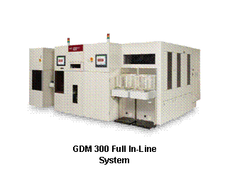
ALBANY, NY | Posted on September 17th, 2009Okamoto announced today that SEMATECH, the global consortium of chip-makers, has selected Okamoto's GDM300 Backgrinder for processing Through Silicon Via (TSV). The System, a High-Precision wafer thinning tool, will be installed in SEMATECH's 3D R&D Center at the College of Nanoscale Science and Engineering's (CNSE) world-class Albany NanoTech Complex.
After the grind process, stress release is achieved by dual high speed scanning polishing heads able to achieve +/- 5% non-uniformity. Improved die strength is achieved by simultaneously utilizing CMP and water polish. An integrated edge trimmer eliminates edge chipping and improves yield. Non-contact measurement devices enable precision thickness accuracy.
Sitaram Arkalgud, SEMATECH's 3D program director, added, "SEMATECH's 3D program is focused on enabling the manufacturability of 3D interconnects, and one of our key infrastructure requirements is a system that provides an integrated process that allows our engineers to identify and quantify the technical challenges of thinning wafer pairs to achieve damage-free bonds."
Richard Brilla, CNSE's Vice President for Strategy, Alliances and Consortia, said, "The addition of Okamoto's wafer-thinning tool will support the advanced work being done through SEMATECH's 3D program, as well as the state-of-the-art capabilities at CNSE's Albany NanoTech, which are enhancing the industry's efforts to manufacture increasingly complex nanoscale devices."
The system is designed for thin wafer applications such as TSV, bonded wafers, SOI, and MEMS. Also available optionally in a full line system for single wafer thinning are dicing frame mounting, UV curing and detaping of protective tape. DAF tape can also be applied in lieu of standard dicing tape.
####
For more information, please click here
Contacts:
Erica McGill
SEMATECH | Media Relations
257 Fuller Road | Suite 2200 | Albany, NY | 12203
o: 518-649-1041 | m: 518-487-8256
Issuers of news releases, not 7th Wave, Inc. or Nanotechnology Now, are solely responsible for the accuracy of the content.
Bookmark:


| Related News Press |
News and information
![]() Quantum computer improves AI predictions April 17th, 2026
Quantum computer improves AI predictions April 17th, 2026
![]() Flexible sensor gains sensitivity under pressure April 17th, 2026
Flexible sensor gains sensitivity under pressure April 17th, 2026
![]() A reusable chip for particulate matter sensing April 17th, 2026
A reusable chip for particulate matter sensing April 17th, 2026
![]() Detecting vibrational quantum beating in the predissociation dynamics of SF6 using time-resolved photoelectron spectroscopy April 17th, 2026
Detecting vibrational quantum beating in the predissociation dynamics of SF6 using time-resolved photoelectron spectroscopy April 17th, 2026
Academic/Education
![]() Rice University launches Rice Synthetic Biology Institute to improve lives January 12th, 2024
Rice University launches Rice Synthetic Biology Institute to improve lives January 12th, 2024
![]() Multi-institution, $4.6 million NSF grant to fund nanotechnology training September 9th, 2022
Multi-institution, $4.6 million NSF grant to fund nanotechnology training September 9th, 2022
Chip Technology
![]() A reusable chip for particulate matter sensing April 17th, 2026
A reusable chip for particulate matter sensing April 17th, 2026
![]() Metasurfaces smooth light to boost magnetic sensing precision January 30th, 2026
Metasurfaces smooth light to boost magnetic sensing precision January 30th, 2026
Announcements
![]() A fundamentally new therapeutic approach to cystic fibrosis: Nanobody repairs cellular defect April 17th, 2026
A fundamentally new therapeutic approach to cystic fibrosis: Nanobody repairs cellular defect April 17th, 2026
![]() UC Irvine physicists discover method to reverse �quantum scrambling� : The work addresses the problem of information loss in quantum computing system April 17th, 2026
UC Irvine physicists discover method to reverse �quantum scrambling� : The work addresses the problem of information loss in quantum computing system April 17th, 2026
Tools
![]() Metasurfaces smooth light to boost magnetic sensing precision January 30th, 2026
Metasurfaces smooth light to boost magnetic sensing precision January 30th, 2026
![]() From sensors to smart systems: the rise of AI-driven photonic noses January 30th, 2026
From sensors to smart systems: the rise of AI-driven photonic noses January 30th, 2026
![]() Japan launches fully domestically produced quantum computer: Expo visitors to experience quantum computing firsthand August 8th, 2025
Japan launches fully domestically produced quantum computer: Expo visitors to experience quantum computing firsthand August 8th, 2025
New-Contracts/Sales/Customers
![]() Bruker Light-Sheet Microscopes at Major Comprehensive Cancer Center: New Advanced Imaging Center Powered by Two MuVi and LCS SPIM Microscopes March 25th, 2021
Bruker Light-Sheet Microscopes at Major Comprehensive Cancer Center: New Advanced Imaging Center Powered by Two MuVi and LCS SPIM Microscopes March 25th, 2021
![]() Arrowhead Pharmaceuticals Announces Closing of Agreement with Takeda November 27th, 2020
Arrowhead Pharmaceuticals Announces Closing of Agreement with Takeda November 27th, 2020
![]() Veeco Announces Aledia Order of 300mm MOCVD Equipment for microLED Displays: Propel� Platform First 300mm System with EFEM Designed for Advanced Display Applications October 20th, 2020
Veeco Announces Aledia Order of 300mm MOCVD Equipment for microLED Displays: Propel� Platform First 300mm System with EFEM Designed for Advanced Display Applications October 20th, 2020
![]() GREENWAVES TECHNOLOGIES Announces Next Generation GAP9 Hearables Platform Using GLOBALFOUNDRIES 22FDX Solution October 16th, 2020
GREENWAVES TECHNOLOGIES Announces Next Generation GAP9 Hearables Platform Using GLOBALFOUNDRIES 22FDX Solution October 16th, 2020
|
|
||
|
|
||
| The latest news from around the world, FREE | ||
|
|
||
|
|
||
| Premium Products | ||
|
|
||
|
Only the news you want to read!
Learn More |
||
|
|
||
|
Full-service, expert consulting
Learn More |
||
|
|
||