Home > Press > Novellus' 32nm UV-Absorbing Dielectric Films Key to Improved Device Reliability
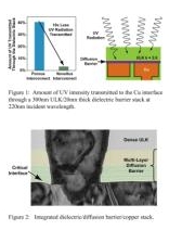 |
| Figure 1: Amount of UV intensity transmitted to the Cu interface through a 300nm ULK/20nm thick dielectric barrier stack at 220nm incident wavelength. Figure 2: Integrated dielectric/diffusion barrier/copper stack. (PRNewsFoto/Novellus Systems, Inc.) |
Abstract:
Dense ULK and Diffusion Barrier Stack Absorbs Order-of-Magnitude More UV Radiation Than Porous Interconnect Alternatives
Novellus' 32nm UV-Absorbing Dielectric Films Key to Improved Device Reliability
San Jose, CA | Posted on May 6th, 2009In order for RC delay to continue to scale in accordance with the International Technology Roadmap for Semiconductors (ITRS), device manufacturers are integrating ultra-low k (ULK) dielectric materials into their 32 nm process flows. At the same time, UltraViolet Thermal Processing (UVTP) is being introduced into the semiconductor manufacturing process to improve the mechanical properties of these ULK materials, making them more robust for subsequent Chemical Mechanical Planarization (CMP) and packaging operations. However, the UVTP process can alter the nature of the stress of the ULK film stack at the copper-dielectric interface. While it is widely accepted that maintaining a compressive stress at this interface can positively impact copper electromigration and film stack reliability, exposing some dielectric films to UV radiation can shift the stress in the film from compressive to tensile, which will negatively affect device performance.
Novellus (Nasdaq: NVLS) has developed a suite of 32nm dielectric films which significantly reduce the transmission of UV radiation to the critical copper-dielectric interface, maintaining a compressive stress in this region and hence device reliability. Figure 1 shows that the Novellus interconnect stack, consisting of a dense ULK and a low-k diffusion barrier, transmits an order-of-magnitude lower UV intensity (220nm wavelength) in comparison to a porous ULK solution. The improved UV absorption of Novellus' ULK film stack is a direct result of the chemical composition of the film. Figure 2 shows the integration of a multi-layer diffusion barrier beneath the dense ULK film. This unique barrier was designed to remain compressive after UV exposure and protect the copper-dielectric interface. Novellus' Multi-Station Sequential Processing (MSSP) architecture ensures that the multi-layer barrier can be deposited in a single pass with high productivity.
"Some 32nm ULK inter-metal dielectric and diffusion barrier films can be negatively impacted by UVTP, changing the stress on the underlying copper-dielectric interface," said Andy Antonelli, technology manager at Novellus' PECVD business. "Relative to competitive offerings, the greater UV absorption capabilities of the new Novellus films preserves the compressive stress at this critical interface and thus minimizes reliability concerns."
For more information regarding the use of dielectric diffusion barriers resistant to UV, go to www.novellustechnews.com.
About Novellus' PECVD Technology:
For high-volume manufacturing applications at 45nm and beyond, Novellus' advanced low-k, ILD, IMD, and dielectric diffusion barrier films offer the lowest k-effective, superior RC control, and an easily integrated low-cost dielectric solution.
####
About Novellus Systems, Inc.
Novellus Systems, Inc. (Nasdaq: NVLS) is a leading provider of advanced process equipment for the global semiconductor industry. The company's products deliver value to customers by providing innovative technology backed by trusted productivity. An S&P 500 company, Novellus is headquartered in San Jose, Calif. with subsidiary offices across the globe.
For more information, please click here
Copyright © PR Newswire Association LLC.
If you have a comment, please Contact us.Issuers of news releases, not 7th Wave, Inc. or Nanotechnology Now, are solely responsible for the accuracy of the content.
Bookmark:


| Related News Press |
News and information
![]() Quantum computer improves AI predictions April 17th, 2026
Quantum computer improves AI predictions April 17th, 2026
![]() Flexible sensor gains sensitivity under pressure April 17th, 2026
Flexible sensor gains sensitivity under pressure April 17th, 2026
![]() A reusable chip for particulate matter sensing April 17th, 2026
A reusable chip for particulate matter sensing April 17th, 2026
![]() Detecting vibrational quantum beating in the predissociation dynamics of SF6 using time-resolved photoelectron spectroscopy April 17th, 2026
Detecting vibrational quantum beating in the predissociation dynamics of SF6 using time-resolved photoelectron spectroscopy April 17th, 2026
Chip Technology
![]() A reusable chip for particulate matter sensing April 17th, 2026
A reusable chip for particulate matter sensing April 17th, 2026
![]() Metasurfaces smooth light to boost magnetic sensing precision January 30th, 2026
Metasurfaces smooth light to boost magnetic sensing precision January 30th, 2026
Announcements
![]() A fundamentally new therapeutic approach to cystic fibrosis: Nanobody repairs cellular defect April 17th, 2026
A fundamentally new therapeutic approach to cystic fibrosis: Nanobody repairs cellular defect April 17th, 2026
![]() UC Irvine physicists discover method to reverse �quantum scrambling� : The work addresses the problem of information loss in quantum computing system April 17th, 2026
UC Irvine physicists discover method to reverse �quantum scrambling� : The work addresses the problem of information loss in quantum computing system April 17th, 2026
Tools
![]() Metasurfaces smooth light to boost magnetic sensing precision January 30th, 2026
Metasurfaces smooth light to boost magnetic sensing precision January 30th, 2026
![]() From sensors to smart systems: the rise of AI-driven photonic noses January 30th, 2026
From sensors to smart systems: the rise of AI-driven photonic noses January 30th, 2026
![]() Japan launches fully domestically produced quantum computer: Expo visitors to experience quantum computing firsthand August 8th, 2025
Japan launches fully domestically produced quantum computer: Expo visitors to experience quantum computing firsthand August 8th, 2025
|
|
||
|
|
||
| The latest news from around the world, FREE | ||
|
|
||
|
|
||
| Premium Products | ||
|
|
||
|
Only the news you want to read!
Learn More |
||
|
|
||
|
Full-service, expert consulting
Learn More |
||
|
|
||