Home > Press > Researchers Find Better Way to Manufacture Fast Computer Chips
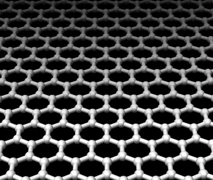 |
| Graphene is an atomic-scale honeycomb lattice made of carbon atoms. Source: Wikipedia. |
Abstract:
Engineers at Ohio State University are developing a technique for mass producing computer chips made from the same material found in pencils.
Researchers Find Better Way to Manufacture Fast Computer Chips
Columbus, OH | Posted on March 31st, 2009Experts believe that graphene -- the sheet-like form of carbon found in graphite pencils -- holds the key to smaller, faster electronics. It might also deliver quantum mechanical effects that could enable new kinds of electronics.
Until now, most researchers could only create tiny graphene devices one at a time, and only on traditional silicon oxide substrates. They couldn't control where they placed the devices on the substrate, and had to connect them to other electronics one at a time for testing.
In a paper published in the March 26 issue of the journal Advanced Materials, Nitin Padture and his colleagues describe a technique for stamping many graphene sheets onto a substrate at once, in precise locations.
"We designed the technique to mesh with standard chip-making practices," said Padture, College of Engineering Distinguished Professor in Materials Science and Engineering.
"Graphene has huge potential -- it's been dubbed �the new silicon,'" said Padture, who is also director of Ohio State's Center for Emergent Materials. "But there hasn't been a good process for high-throughput manufacturing it into chips. The industry has several decades of chip-making technology that we can tap into, if only we could create millions of these graphene structures in precise patterns on predetermined locations, repeatedly. This result is a proof-of-concept that we should be able to do just that."
Graphene is made of carbon atoms arranged in a hexagonal pattern resembling chicken wire. In graphite, many flat graphene sheets are stacked together.
"When you write with a pencil, you leave graphene sheets behind on the paper," Padture said. Each sheet is so thin -- a few tenths of a nanometer (billionths of a meter) -- that researchers think of it as a two-dimensional crystal.
Researchers have shown that a single sheet, or even a few sheets, of graphene can exhibit special properties. One such property is very high mobility, in which electrons can pass through it very quickly -- a good characteristic for fast electronics. Another is magnetism: magnetic fields could be used to control the spin of graphene electrons, which would enable spin-based electronics, also called spintronics.
Yet another characteristic is how dramatically graphene's properties change when it touches other materials. That makes it a good candidate material for chemical sensors.
In this method, Padture and his Ohio State colleagues carved graphite into different shapes -- a field of microscopic pillars, for example -- and then stamped the shapes onto silicon oxide surfaces.
"Think of a stack of graphene sheets in graphite as a deck of cards. When you bring it contact with the silicon oxide and pull it away, you can �split the deck' near the point of contact, leaving some layers of graphene behind. What we found through computer simulations was that the graphene surface interacts so strongly with the silicon oxide surface that the chemical bonds between the graphene layers weaken, and the lower layers split off," Padture said.
In this first series of experiments, the Ohio State researchers were able to stamp high-definition features that were ten layers thick, or thicker. The graphite stamp can then be used repeatedly on other predetermined locations on the same or other substrates, making this a mass-production method, potentially.
They used three different kinds of microscopes -- a scanning electron microscope, optical microscope, and atomic force microscope -- to measure the heights of the features, and assure that they were placed precisely on the substrate.
They eventually hope to stamp narrow features that are only one or two layers thick, by stamping on materials other than silicon oxide.
In computer simulations, they found that each material interacts differently with the graphene. So success might rely on finding just the right combination of substrate materials to coax the graphene to break off in one or two layers. This would also tailor the properties of the graphene.
Padture's co-authors on the paper include Dongsheng Li, a postdoctoral researcher, and Wolfgang Windl, associate professor of materials science and engineering.
This work was partially funded by the Center for Emergent Materials at Ohio State, which is a Materials Research Science & Engineering Center (MRSEC) sponsored by the National Science Foundation. The $17-million center is one of only 27 MRSECs (www.mrsec.org) around the country, and its main research focus is magnetoelectronics. Partial funding was also provided by Ohio State's Institute for Materials Research.
####
For more information, please click here
Contacts:
Nitin Padture
(614) 247-8114
Written by Pam Frost Gorder
(614) 292-9475
Copyright © Ohio State University
If you have a comment, please Contact us.Issuers of news releases, not 7th Wave, Inc. or Nanotechnology Now, are solely responsible for the accuracy of the content.
Bookmark:


| Related News Press |
News and information
![]() Quantum computer improves AI predictions April 17th, 2026
Quantum computer improves AI predictions April 17th, 2026
![]() Flexible sensor gains sensitivity under pressure April 17th, 2026
Flexible sensor gains sensitivity under pressure April 17th, 2026
![]() A reusable chip for particulate matter sensing April 17th, 2026
A reusable chip for particulate matter sensing April 17th, 2026
![]() Detecting vibrational quantum beating in the predissociation dynamics of SF6 using time-resolved photoelectron spectroscopy April 17th, 2026
Detecting vibrational quantum beating in the predissociation dynamics of SF6 using time-resolved photoelectron spectroscopy April 17th, 2026
Possible Futures
![]() A fundamentally new therapeutic approach to cystic fibrosis: Nanobody repairs cellular defect April 17th, 2026
A fundamentally new therapeutic approach to cystic fibrosis: Nanobody repairs cellular defect April 17th, 2026
![]() UC Irvine physicists discover method to reverse �quantum scrambling� : The work addresses the problem of information loss in quantum computing system April 17th, 2026
UC Irvine physicists discover method to reverse �quantum scrambling� : The work addresses the problem of information loss in quantum computing system April 17th, 2026
Chip Technology
![]() A reusable chip for particulate matter sensing April 17th, 2026
A reusable chip for particulate matter sensing April 17th, 2026
![]() Metasurfaces smooth light to boost magnetic sensing precision January 30th, 2026
Metasurfaces smooth light to boost magnetic sensing precision January 30th, 2026
Quantum Computing
![]() Quantum computer improves AI predictions April 17th, 2026
Quantum computer improves AI predictions April 17th, 2026
![]() UC Irvine physicists discover method to reverse �quantum scrambling� : The work addresses the problem of information loss in quantum computing system April 17th, 2026
UC Irvine physicists discover method to reverse �quantum scrambling� : The work addresses the problem of information loss in quantum computing system April 17th, 2026
![]() Researchers develop molecular qubits that communicate at telecom frequencies October 3rd, 2025
Researchers develop molecular qubits that communicate at telecom frequencies October 3rd, 2025
Nanoelectronics
![]() Lab to industry: InSe wafer-scale breakthrough for future electronics August 8th, 2025
Lab to industry: InSe wafer-scale breakthrough for future electronics August 8th, 2025
![]() Interdisciplinary: Rice team tackles the future of semiconductors Multiferroics could be the key to ultralow-energy computing October 6th, 2023
Interdisciplinary: Rice team tackles the future of semiconductors Multiferroics could be the key to ultralow-energy computing October 6th, 2023
![]() Key element for a scalable quantum computer: Physicists from Forschungszentrum J�lich and RWTH Aachen University demonstrate electron transport on a quantum chip September 23rd, 2022
Key element for a scalable quantum computer: Physicists from Forschungszentrum J�lich and RWTH Aachen University demonstrate electron transport on a quantum chip September 23rd, 2022
![]() Reduced power consumption in semiconductor devices September 23rd, 2022
Reduced power consumption in semiconductor devices September 23rd, 2022
Discoveries
![]() Quantum computer improves AI predictions April 17th, 2026
Quantum computer improves AI predictions April 17th, 2026
![]() Flexible sensor gains sensitivity under pressure April 17th, 2026
Flexible sensor gains sensitivity under pressure April 17th, 2026
![]() A reusable chip for particulate matter sensing April 17th, 2026
A reusable chip for particulate matter sensing April 17th, 2026
![]() Detecting vibrational quantum beating in the predissociation dynamics of SF6 using time-resolved photoelectron spectroscopy April 17th, 2026
Detecting vibrational quantum beating in the predissociation dynamics of SF6 using time-resolved photoelectron spectroscopy April 17th, 2026
Announcements
![]() A fundamentally new therapeutic approach to cystic fibrosis: Nanobody repairs cellular defect April 17th, 2026
A fundamentally new therapeutic approach to cystic fibrosis: Nanobody repairs cellular defect April 17th, 2026
![]() UC Irvine physicists discover method to reverse �quantum scrambling� : The work addresses the problem of information loss in quantum computing system April 17th, 2026
UC Irvine physicists discover method to reverse �quantum scrambling� : The work addresses the problem of information loss in quantum computing system April 17th, 2026
|
|
||
|
|
||
| The latest news from around the world, FREE | ||
|
|
||
|
|
||
| Premium Products | ||
|
|
||
|
Only the news you want to read!
Learn More |
||
|
|
||
|
Full-service, expert consulting
Learn More |
||
|
|
||