Home > Press > SUSS MicroTec launches 300mm Coat/Develop Cluster enhanced for 3D Integration
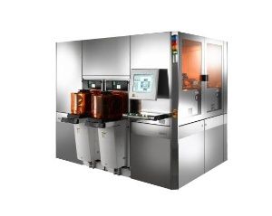 |
| Frontview ACS300 Gen2 modular coat/bake/develop system from SUSS MicroTec (Photo: Business Wire) |
Abstract:
At Semicon Korea 2009, SUSS MicroTec (FWB:SMH)(GER:SMH) unveiled the second generation of its ACS300, a modular system for coating, baking and developing of wafers up to 300mm. The ACS300 Gen2 offers unmatched configuration flexibility at market-leading cost of ownership. The system architecture and process modules are specifically adapted to the needs of the advanced packaging and 3D integration industry, which requires very thick photo resist layers of up to 100 microns and more. Combining best in class coat and develop uniformity with exceptional edge bead performance makes the ACS300 Gen2 the preferred solution for various special spin coating applications such photosensitive polymers like polyimide, PBO or Cyclotene™ (BCB).
SUSS MicroTec launches 300mm Coat/Develop Cluster enhanced for 3D Integration
MUNICH, Germany | Posted on January 19th, 2009 The ACS300 Gen2 continues the success of the preceding model, ACS300Plus with developments driving equipment cost down, extending overall equipment efficiency and scaling down of the footprint.
"Addressing the specific requirements for wafer level packaging and 3D integration the new ACS300 is equipped with various packaging specific features, which makes it specifically suited for applications like solder bumping, gold bumping or redistribution layers," said Rolf Wolf, General Manager of SUSS MicroTec Lithography Division. "The next generation ACS300 will definitively help SUSS MicroTec to continue and further expand its market leading position in the field of advanced packaging, and extending it into 3D processing."
####
About SUSS MicroTec
SUSS MicroTec is a leading supplier of process and test solutions for markets such as 3D Integration, Advanced Packaging, MEMS, Nanotechnology and Compound Semiconductor. High-quality solutions enable customers to increase process performance while reducing cost of ownership.
SUSS MicroTec supports more than 8,000 installed mask aligners, coaters, bonders and probe systems with a global infrastructure for applications and service. SUSS MicroTec is headquartered in Garching near Munich, Germany.
All statements in this release other than historical facts are forward-looking statements within the meaning of U.S. Private Securities Litigation Reform Act of 1995. The company accepts no obligation toward the general public to update or correct forward-looking statements. All forward-looking statements are subject to various risks and uncertainties, as a result of which actual events may diverge numerically from expectations. The forward-looking statements reflect the view at the time they were made.
For more information, please click here
Contacts:
SUSS MicroTec
Brigitte Wehrmann
Marketing Communications Manager
SUSS MicroTec Lithography Division
Tel: +49 (0) 89 32007-237
Copyright © Business Wire 2009
If you have a comment, please Contact us.Issuers of news releases, not 7th Wave, Inc. or Nanotechnology Now, are solely responsible for the accuracy of the content.
Bookmark:


| Related News Press |
News and information
![]() Quantum computer improves AI predictions April 17th, 2026
Quantum computer improves AI predictions April 17th, 2026
![]() Flexible sensor gains sensitivity under pressure April 17th, 2026
Flexible sensor gains sensitivity under pressure April 17th, 2026
![]() A reusable chip for particulate matter sensing April 17th, 2026
A reusable chip for particulate matter sensing April 17th, 2026
![]() Detecting vibrational quantum beating in the predissociation dynamics of SF6 using time-resolved photoelectron spectroscopy April 17th, 2026
Detecting vibrational quantum beating in the predissociation dynamics of SF6 using time-resolved photoelectron spectroscopy April 17th, 2026
Chip Technology
![]() A reusable chip for particulate matter sensing April 17th, 2026
A reusable chip for particulate matter sensing April 17th, 2026
![]() Metasurfaces smooth light to boost magnetic sensing precision January 30th, 2026
Metasurfaces smooth light to boost magnetic sensing precision January 30th, 2026
Announcements
![]() A fundamentally new therapeutic approach to cystic fibrosis: Nanobody repairs cellular defect April 17th, 2026
A fundamentally new therapeutic approach to cystic fibrosis: Nanobody repairs cellular defect April 17th, 2026
![]() UC Irvine physicists discover method to reverse ‘quantum scrambling’ : The work addresses the problem of information loss in quantum computing system April 17th, 2026
UC Irvine physicists discover method to reverse ‘quantum scrambling’ : The work addresses the problem of information loss in quantum computing system April 17th, 2026
Tools
![]() Metasurfaces smooth light to boost magnetic sensing precision January 30th, 2026
Metasurfaces smooth light to boost magnetic sensing precision January 30th, 2026
![]() From sensors to smart systems: the rise of AI-driven photonic noses January 30th, 2026
From sensors to smart systems: the rise of AI-driven photonic noses January 30th, 2026
![]() Japan launches fully domestically produced quantum computer: Expo visitors to experience quantum computing firsthand August 8th, 2025
Japan launches fully domestically produced quantum computer: Expo visitors to experience quantum computing firsthand August 8th, 2025
|
|
||
|
|
||
| The latest news from around the world, FREE | ||
|
|
||
|
|
||
| Premium Products | ||
|
|
||
|
Only the news you want to read!
Learn More |
||
|
|
||
|
Full-service, expert consulting
Learn More |
||
|
|
||