Home > Press > Insights into Polymer Film Instability Could Aid High Tech Industries
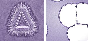 |
| Crystallization (left) occurs as polymers harden into thin films, which are used widely in electronics technology. But when dewetting (right) also occurs, inhomogeneities in the film can degrade performance. NIST scientists found that temperature determines which process dominates film formation, and that keeping certain angles between crystallization fronts can largely prevent dewetting.
Credit: NIST |
Abstract:
While exploring the properties of polymer formation, a team of scientists at the National Institute for Standards and Technology (NIST) has made a fundamental discovery* about these materials that could improve methods of creating the stable crystalline films that are widely used in electronics applications—and also offer insight into a range of other phenomena.
Insights into Polymer Film Instability Could Aid High Tech Industries
GAITHERSBURG, MD | Posted on January 13th, 2009The team has determined that temperature can play a decisive role in determining which of two competing processes—called crystallization and dewetting—will "take the lead" when a semicrystalline polymer film hardens, thereby granting qualitatively different properties to the finished film. The findings could lead to better control of these two processes, which can cause imperfections in polymer films during their formation.
Such imperfections can hinder the performance of potential new technologies, such as solar cells or thin film transistors, that employ organic polymer films on their surfaces, according to research chemist Christopher Soles. At this point, he said, the organic semiconductor industry is being hindered by a lack of understanding of crystal formation in thin polymer films.
"If organic photovoltaics—to take just one example—are ever to be realized and marketed, we need to understand how the film formation process works," said Soles. "You have to know the properties of these materials first in order to control their stability."
As a polymer film cools, two different things can happen locally within it: Either its molecules can crystallize, starting from some nucleation center (such as a scratch) and then expanding into the surrounding unstable film. Or, because of chemical differences between the polymer and its underlying substrate, such as a silicon wafer, the film's molecules can "dewet"—similar to the beading up of water droplets on a windshield. If crystallization and dewetting occur simultaneously, they can couple to create imperfections that can be a nuisance for applications that rely on film uniformity, such as organic solar cells. The challenge is to bring these instabilities under control for constructive purposes.
Using model polymers with well understood crystallization behavior, the team discovered that a few degrees' variation in temperature controls whether crystallization or dewetting will dominate the hardening process. They also found that when two growing crystals expand and collide, the stress created where they contact each other can cause dewetting—but if the angle between the two expansion fronts is small enough, then this localized dewetting might be averted.
"What's cool about this discovery is not just that we have better understanding of polymer films, which are widely used in a range of coating and interface technologies," said coauthor Jack Douglas, also of NIST's polymers division. "There's a whole class of mathematical problems in which you have multiple effects that are all fighting for domination of some field of action—the spreading of languages, for example, or the growth of different tissues within organisms. It's a very common phenomenon, and this research could provide theoretical insight into those problems as well."
Funding for this study was provided by the National Research Council.
* B.C. Okerberg, B.C. Berry, T.R. Garvey, J.F. Douglas, A. Karim and C.L. Soles. Competition between crystallization and dewetting fronts in this polymer films. Soft Matter, November 2008, 1-7. DOI: 10.1039/b806074f
####
About NIST
Founded in 1901, NIST is a non-regulatory federal agency within the U.S. Department of Commerce. NIST's mission is to promote U.S. innovation and industrial competitiveness by advancing measurement science, standards, and technology in ways that enhance economic security and improve our quality of life.
For more information, please click here
Contacts:
Chad Boutin
(301) 975-4261
Copyright © NIST
If you have a comment, please Contact us.Issuers of news releases, not 7th Wave, Inc. or Nanotechnology Now, are solely responsible for the accuracy of the content.
Bookmark:


| Related News Press |
News and information
![]() Quantum computer improves AI predictions April 17th, 2026
Quantum computer improves AI predictions April 17th, 2026
![]() Flexible sensor gains sensitivity under pressure April 17th, 2026
Flexible sensor gains sensitivity under pressure April 17th, 2026
![]() A reusable chip for particulate matter sensing April 17th, 2026
A reusable chip for particulate matter sensing April 17th, 2026
![]() Detecting vibrational quantum beating in the predissociation dynamics of SF6 using time-resolved photoelectron spectroscopy April 17th, 2026
Detecting vibrational quantum beating in the predissociation dynamics of SF6 using time-resolved photoelectron spectroscopy April 17th, 2026
Chip Technology
![]() A reusable chip for particulate matter sensing April 17th, 2026
A reusable chip for particulate matter sensing April 17th, 2026
![]() Metasurfaces smooth light to boost magnetic sensing precision January 30th, 2026
Metasurfaces smooth light to boost magnetic sensing precision January 30th, 2026
Discoveries
![]() Quantum computer improves AI predictions April 17th, 2026
Quantum computer improves AI predictions April 17th, 2026
![]() Flexible sensor gains sensitivity under pressure April 17th, 2026
Flexible sensor gains sensitivity under pressure April 17th, 2026
![]() A reusable chip for particulate matter sensing April 17th, 2026
A reusable chip for particulate matter sensing April 17th, 2026
![]() Detecting vibrational quantum beating in the predissociation dynamics of SF6 using time-resolved photoelectron spectroscopy April 17th, 2026
Detecting vibrational quantum beating in the predissociation dynamics of SF6 using time-resolved photoelectron spectroscopy April 17th, 2026
Announcements
![]() A fundamentally new therapeutic approach to cystic fibrosis: Nanobody repairs cellular defect April 17th, 2026
A fundamentally new therapeutic approach to cystic fibrosis: Nanobody repairs cellular defect April 17th, 2026
![]() UC Irvine physicists discover method to reverse ‘quantum scrambling’ : The work addresses the problem of information loss in quantum computing system April 17th, 2026
UC Irvine physicists discover method to reverse ‘quantum scrambling’ : The work addresses the problem of information loss in quantum computing system April 17th, 2026
|
|
||
|
|
||
| The latest news from around the world, FREE | ||
|
|
||
|
|
||
| Premium Products | ||
|
|
||
|
Only the news you want to read!
Learn More |
||
|
|
||
|
Full-service, expert consulting
Learn More |
||
|
|
||