Home > Press > Applied Materials Delivers Critical Copper Barrier Technology for Memory Chips with Extensa PVD System
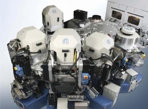 |
| The Applied Endura Extensa PVD system's unique titanium/titanium nitride process technology delivers the essential barrier films needed for fabricating copper interconnects in sub-55nm memory chips. (Photo: Business Wire) |
Abstract:
Applied Materials, Inc. today announced its Applied Endura® Extensa™ PVD1, the industry's only production-worthy system for depositing the critical barrier films for copper interconnects in sub-55nm memory chips. The Extensa system's unique titanium/titanium nitride (Ti/TiN) process technology enables diffusion barrier films with benchmark step coverage and <3% film thickness non-uniformity across the wafer, while achieving best-in-class defectivity and >25% lower CoC2 than competing systems.
Applied Materials Delivers Critical Copper Barrier Technology for Memory Chips with Extensa PVD System
SANTA CLARA, CA | Posted on July 15th, 2008 "The introduction of copper in memory devices presents unique film integration challenges due to the high voltages and dense packing requirements of memory cells," said Prabu Raja, vice president and general manager of Applied's Metal Deposition Products division. "Manufacturers are adopting new liner/barrier schemes as the most cost-effective way to get the performance benefits of copper. The Extensa system enables the robust integration of these critical new diffusion barriers with a proven, single-system solution that allows memory makers to realize high device yields down to the 32nm technology node and beyond."
The Applied Extensa system's outstanding performance, already proven at multiple customer sites, is the result of several innovations in PVD technology that are implemented on the Extensa Ti/TiN deposition chamber. A novel dual-magnet PVD source with flux-shaping side electromagnets enables unmatched step coverage and defectivity below 10 particles at ≥0.12 micrometer. The proprietary source technology also makes more efficient use of deposition material, delivering a 30% improvement in target life. In addition, the single piece chamber kit features Applied's proprietary CleanCoat™ technology for ease of maintenance and particle control.
Integrated on the highly successful Applied Endura platform, the Extensa technology offers Ti/TiN deposition solutions to support two key technology transitions in memory: the replacement of tantalum with Ti-based dielectric barriers in copper barrier/seed applications, and the introduction of copper-aluminum and copper-tungsten diffusion barriers that enable the most cost effective integration of copper with aluminum layers and tungsten vias.
Additional applications include contact liner for memory devices and, for logic customers, metal gate and silicide cap barrier deposition. The unique flexibility of the Endura architecture enables the industry's only integrated copper-aluminum barrier and aluminum fill solution on a single system. For more information, visit appliedmaterials.com/products/endura_extensa.html.
1 PVD = physical vapor deposition
2 CoC = cost of consumables
####
About Applied Materials, Inc.
Applied Materials, Inc. (Nasdaq:AMAT) is the global leader in Nanomanufacturing Technology™ solutions with a broad portfolio of innovative equipment, service and software products for the fabrication of semiconductor chips, flat panel displays, solar photovoltaic cells, flexible electronics and energy efficient glass. At Applied Materials, we apply Nanomanufacturing Technology to improve the way people live.
For more information, please click here
Contacts:
Applied Materials, Inc.
Betty Newboe
408-563-0647 (editorial/media)
Linda Heller
408-986-7977 (financial community)
Copyright © Business Wire 2008
If you have a comment, please Contact us.Issuers of news releases, not 7th Wave, Inc. or Nanotechnology Now, are solely responsible for the accuracy of the content.
Bookmark:


| Related News Press |
News and information
![]() Quantum computer improves AI predictions April 17th, 2026
Quantum computer improves AI predictions April 17th, 2026
![]() Flexible sensor gains sensitivity under pressure April 17th, 2026
Flexible sensor gains sensitivity under pressure April 17th, 2026
![]() A reusable chip for particulate matter sensing April 17th, 2026
A reusable chip for particulate matter sensing April 17th, 2026
![]() Detecting vibrational quantum beating in the predissociation dynamics of SF6 using time-resolved photoelectron spectroscopy April 17th, 2026
Detecting vibrational quantum beating in the predissociation dynamics of SF6 using time-resolved photoelectron spectroscopy April 17th, 2026
Chip Technology
![]() A reusable chip for particulate matter sensing April 17th, 2026
A reusable chip for particulate matter sensing April 17th, 2026
![]() Metasurfaces smooth light to boost magnetic sensing precision January 30th, 2026
Metasurfaces smooth light to boost magnetic sensing precision January 30th, 2026
Announcements
![]() A fundamentally new therapeutic approach to cystic fibrosis: Nanobody repairs cellular defect April 17th, 2026
A fundamentally new therapeutic approach to cystic fibrosis: Nanobody repairs cellular defect April 17th, 2026
![]() UC Irvine physicists discover method to reverse ‘quantum scrambling’ : The work addresses the problem of information loss in quantum computing system April 17th, 2026
UC Irvine physicists discover method to reverse ‘quantum scrambling’ : The work addresses the problem of information loss in quantum computing system April 17th, 2026
Tools
![]() Metasurfaces smooth light to boost magnetic sensing precision January 30th, 2026
Metasurfaces smooth light to boost magnetic sensing precision January 30th, 2026
![]() From sensors to smart systems: the rise of AI-driven photonic noses January 30th, 2026
From sensors to smart systems: the rise of AI-driven photonic noses January 30th, 2026
![]() Japan launches fully domestically produced quantum computer: Expo visitors to experience quantum computing firsthand August 8th, 2025
Japan launches fully domestically produced quantum computer: Expo visitors to experience quantum computing firsthand August 8th, 2025
|
|
||
|
|
||
| The latest news from around the world, FREE | ||
|
|
||
|
|
||
| Premium Products | ||
|
|
||
|
Only the news you want to read!
Learn More |
||
|
|
||
|
Full-service, expert consulting
Learn More |
||
|
|
||