Home > Press > Carl Zeiss SMT Opens New North American Headquarters
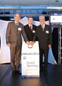 |
| Open for Business! With a push of the button, Dr. Dirk Stenkamp and Frank Averdung (Carl Zeiss) and Dr. Bernd Rinner (Deputy Consul Gen-eral, German Consulate, Boston) started the "Nano-Ribbon Cutting" cere-mony to officially open the new Carl Zeiss SMT North American Head-quarters in Peabody, Massachusetts. (Photo: Business Wire) |
Abstract:
Combined Production, Service and Demo Facility will be cornerstone of growth strategy in the Nanotechnology Market
Carl Zeiss SMT Opens New North American Headquarters
PEABODY, MA | Posted on April 23rd, 2008Carl Zeiss SMT, a leading global provider of electron- and ion-beam imaging and analysis solutions, today officially opened its new North American headquarters in Peabody, Mass., near Boston. Representing an investment of more than nine million dollars, the new 53,000 square foot facility houses the research, development and production center for the unique ORION� helium ion microscope product line. In addition, the facility serves as the North American hub for sales and service for the complete family of ZEISS particle beam instruments and houses the Carl Zeiss Nano Solutions Center Peabody. This center is a comprehensive demonstration and application development facility hosting six of the latest generation electron- and ion-beam systems for nanoscale imaging, analysis and structuring.
Dirk Stenkamp, member of the board of Carl Zeiss SMT, emphasized in his grand opening address: "North America has positioned itself at the forefronts of nanotechnology for advanced materials, life sciences and semiconductor research and development. With our major investments in the new Peabody facility and its highly skilled staff for research, development, production, sales, marketing and services, we are directly addressing the increasing needs and expectations of our North American customers. The new Peabody facility will be a cornerstone of our worldwide growth strategy in the markets for nanotechnology."
Frank P. Averdung, President of Carl Zeiss SMT Inc., explained what this means to the Carl Zeiss SMT customers: "With the completion of our new Peabody facility, we are better positioned than ever to provide a world class experience in nanoscale imaging, analysis and structuring for our North American customers�from academia to research and a wide array of industries. This includes joint research and development programs, applications development, sales and customer service and support activities."
Home office for 150 employees and a breakthrough technology
The new Peabody headquarters represents the home office for more than 150 highly skilled employees and a number of unique microscope technologies including the novel ZEISS ORION� helium ion microscope. This technology will give researchers all over the world the opportunity to image and analyze a wide variety of materials and specimens with unequaled sub-nanometer resolution, depth of field and material contrast. In this way, the innovative power and expertise of Carl Zeiss SMT will continue to enable major advancements in materials research, life sciences and semiconductor manufacturing.
The first customers to use the new ORION� technology include the National Institute of Standards and Technology (NIST) in Gaithersburg, MD, the Center for Nanoscale Systems (CNS) at the Faculty for Arts and Sciences of Harvard University, Boston, and the �Carl Zeiss Innovation Center Dresden�, Germany all striving to develop new breakthrough methods and application results using this revolutionary new type of microscopy.
"We anticipate that we will continue to grow our organization in Peabody, making it the gold standard of customer sales and service for North America," said Averdung. "Being located near Boston, with its world renowned Universities like Harvard and the Massachusetts Institute of Technology provides an ideal cultural and scientific environment to stimulate imaginative and creative thinking for ongoing product and application development."
More information and images are available at www.smt.zeiss.com
PI No. 0082-2008-ENG
April 2008
####
About Carl Zeiss SMT Inc.
Carl Zeiss SMT utilizes its globally leading know-how in light, electron and ion-optical technologies to offer its customers in the manufacturing industry and R&D a broad portfolio of products, services and application solutions. The market-leading systems and solutions from Carl Zeiss SMT are used in mutually strengthening fields of application in nanotechnology such as semiconductor technology, materials research and the life sciences. The global customer community is constantly growing. As the innovation leader for lithography optics, as well as optical and particle-beam based inspection, analysis and measuring systems, Carl Zeiss SMT opens up new avenues for its customers in industrial manufacturing environments, quality assurance and industrial and university R&D. Together with its subsidiaries in Germany, England, France and the USA, the international group of companies has over 2,500 employees. In fiscal year 2006/07, Carl Zeiss SMT AG generated revenues of over EUR 1,000 billion. Carl Zeiss SMT AG is a wholly owned subsidiary of Carl Zeiss AG.
For more information, please click here
Contacts:
Press
Carl Zeiss SMT Inc.
Bill Monigle
941-497-1622
or
Carl Zeiss SMT AG
Markus Wiederspahn
+49 7364 20 2194
Copyright © Business Wire 2008
If you have a comment, please Contact us.Issuers of news releases, not 7th Wave, Inc. or Nanotechnology Now, are solely responsible for the accuracy of the content.
Bookmark:


| Related News Press |
News and information
![]() Quantum computer improves AI predictions April 17th, 2026
Quantum computer improves AI predictions April 17th, 2026
![]() Flexible sensor gains sensitivity under pressure April 17th, 2026
Flexible sensor gains sensitivity under pressure April 17th, 2026
![]() A reusable chip for particulate matter sensing April 17th, 2026
A reusable chip for particulate matter sensing April 17th, 2026
![]() Detecting vibrational quantum beating in the predissociation dynamics of SF6 using time-resolved photoelectron spectroscopy April 17th, 2026
Detecting vibrational quantum beating in the predissociation dynamics of SF6 using time-resolved photoelectron spectroscopy April 17th, 2026
Imaging
![]() Simple algorithm paired with standard imaging tool could predict failure in lithium metal batteries August 8th, 2025
Simple algorithm paired with standard imaging tool could predict failure in lithium metal batteries August 8th, 2025
Openings/New facilities/Groundbreaking/Expansion
![]() OCSiAl expands its graphene nanotube production capacities to Europe June 17th, 2022
OCSiAl expands its graphene nanotube production capacities to Europe June 17th, 2022
![]() GLOBALFOUNDRIES Moves Corporate Headquarters to its Most Advanced Semiconductor Manufacturing Facility in New York April 27th, 2021
GLOBALFOUNDRIES Moves Corporate Headquarters to its Most Advanced Semiconductor Manufacturing Facility in New York April 27th, 2021
![]() Oxford Instruments Plasma Technology relocates to advanced manufacturing facility: Move driven by exceptional business growth February 12th, 2021
Oxford Instruments Plasma Technology relocates to advanced manufacturing facility: Move driven by exceptional business growth February 12th, 2021
Announcements
![]() A fundamentally new therapeutic approach to cystic fibrosis: Nanobody repairs cellular defect April 17th, 2026
A fundamentally new therapeutic approach to cystic fibrosis: Nanobody repairs cellular defect April 17th, 2026
![]() UC Irvine physicists discover method to reverse �quantum scrambling� : The work addresses the problem of information loss in quantum computing system April 17th, 2026
UC Irvine physicists discover method to reverse �quantum scrambling� : The work addresses the problem of information loss in quantum computing system April 17th, 2026
Tools
![]() Metasurfaces smooth light to boost magnetic sensing precision January 30th, 2026
Metasurfaces smooth light to boost magnetic sensing precision January 30th, 2026
![]() From sensors to smart systems: the rise of AI-driven photonic noses January 30th, 2026
From sensors to smart systems: the rise of AI-driven photonic noses January 30th, 2026
![]() Japan launches fully domestically produced quantum computer: Expo visitors to experience quantum computing firsthand August 8th, 2025
Japan launches fully domestically produced quantum computer: Expo visitors to experience quantum computing firsthand August 8th, 2025
|
|
||
|
|
||
| The latest news from around the world, FREE | ||
|
|
||
|
|
||
| Premium Products | ||
|
|
||
|
Only the news you want to read!
Learn More |
||
|
|
||
|
Full-service, expert consulting
Learn More |
||
|
|
||