Home > Press > Visualizing temperature transport: An unexpected technique for nanoscale characterization
 |
| CREDIT Tokyo Tech |
Abstract:
As devices continue to shrink, new challenges in their measurement and design present themselves. For devices based on molecular junctions, in which single molecules are bound to metals or semiconductors, we have a variety of techniques to study and characterize their electric transport properties. In contrast, probing the thermal transport properties of such junctions at the nanoscale has proven more challenging, and many temperature-related quantum phenomena in them remain poorly understood.
Visualizing temperature transport: An unexpected technique for nanoscale characterization
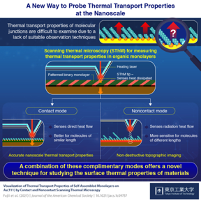
Tokyo, Japan | Posted on November 19th, 2021In a few studies, scientists managed to measure the thermal transport properties in molecular junctions at the nanoscale using a technique called scanning thermal microscopy (SThM). This method involves putting a very sharp metallic tip in contact with the target material and moving this tip throughout the material�s surface. The tip, which is heated from behind using a laser, contains a thermocouple. This small device measures temperature differences and so, by balancing the heating of the tip caused by the laser with the tip�s cooling caused by heat flowing into the target sample, it becomes possible to measure a material�s thermal transport characteristics point by point.
In a recent study published in Journal of the American Chemical Society, scientists from Tokyo Tech reported a serendipitous yet important finding while using SThM. The team was employing a SThM technique to measure the thermal transport properties of self-assembled monolayers (SAMs). These samples contained alternating stripes of each of the three possible pairs between n-Hexadecanethiol, n-Butanethiol, and Benzenethiol. Besides employing the standard contact-based SThM approach, the researchers tried using a non-contact regime as well, in which the tip of the scanning thermal microscope was kept above the sample without touching it. Unexpectedly, they realized this non-contact regime had some serious potential.
In the contact SThM regime, heat flows directly from the tip to the sample. By contrast, in the non-contact SThM regime, the only heat transfer between the tip and the sample occurs via heat radiation. As the team found out through experiments, while the contact regime is best for visualizing the thermal transport characteristics, the non-contact regime is much more sensitive to the actual length of the molecules �sticking out� from the substrate. Thus, the combination of the non-contact and contact regimes provides an all-new way of creating topographic and thermal transport images of a sample simultaneously.
Moreover, the non-contact approach has advantages over other well-established microscopy techniques, as Associate Professor Shintaro Fujii, lead author of the paper, explains: �The non-contact SThM approach is completely non-destructive, unlike other techniques like atomic force microscopy, which does require contact between the scanning tip and the sample and thus has a mechanical impact that can damage soft organic materials.�
Overall, the insight provided by this study will pave the way to novel technological advances and a deeper comprehension of materials at the nanoscale. �Our work not only is the first to provide thermal images of organic SAMs, but also provides a new technique for investigating thermal transport properties, which will be essential for thermal management in various types of nanodevices,� concludes Fujii.
Let us hope this work helps scientists elucidate the many mysteries of thermal phenomena.
####
For more information, please click here
Contacts:
Kazuhide Hasegawa
Tokyo Institute of Technology
Copyright © Tokyo Institute of Technology
If you have a comment, please Contact us.Issuers of news releases, not 7th Wave, Inc. or Nanotechnology Now, are solely responsible for the accuracy of the content.
Bookmark:


| Related Links |
| Related News Press |
News and information
![]() Quantum computer improves AI predictions April 17th, 2026
Quantum computer improves AI predictions April 17th, 2026
![]() Flexible sensor gains sensitivity under pressure April 17th, 2026
Flexible sensor gains sensitivity under pressure April 17th, 2026
![]() A reusable chip for particulate matter sensing April 17th, 2026
A reusable chip for particulate matter sensing April 17th, 2026
![]() Detecting vibrational quantum beating in the predissociation dynamics of SF6 using time-resolved photoelectron spectroscopy April 17th, 2026
Detecting vibrational quantum beating in the predissociation dynamics of SF6 using time-resolved photoelectron spectroscopy April 17th, 2026
Imaging
![]() Simple algorithm paired with standard imaging tool could predict failure in lithium metal batteries August 8th, 2025
Simple algorithm paired with standard imaging tool could predict failure in lithium metal batteries August 8th, 2025
Possible Futures
![]() A fundamentally new therapeutic approach to cystic fibrosis: Nanobody repairs cellular defect April 17th, 2026
A fundamentally new therapeutic approach to cystic fibrosis: Nanobody repairs cellular defect April 17th, 2026
![]() UC Irvine physicists discover method to reverse �quantum scrambling� : The work addresses the problem of information loss in quantum computing system April 17th, 2026
UC Irvine physicists discover method to reverse �quantum scrambling� : The work addresses the problem of information loss in quantum computing system April 17th, 2026
Chip Technology
![]() A reusable chip for particulate matter sensing April 17th, 2026
A reusable chip for particulate matter sensing April 17th, 2026
![]() Metasurfaces smooth light to boost magnetic sensing precision January 30th, 2026
Metasurfaces smooth light to boost magnetic sensing precision January 30th, 2026
Nanoelectronics
![]() Lab to industry: InSe wafer-scale breakthrough for future electronics August 8th, 2025
Lab to industry: InSe wafer-scale breakthrough for future electronics August 8th, 2025
![]() Interdisciplinary: Rice team tackles the future of semiconductors Multiferroics could be the key to ultralow-energy computing October 6th, 2023
Interdisciplinary: Rice team tackles the future of semiconductors Multiferroics could be the key to ultralow-energy computing October 6th, 2023
![]() Key element for a scalable quantum computer: Physicists from Forschungszentrum J�lich and RWTH Aachen University demonstrate electron transport on a quantum chip September 23rd, 2022
Key element for a scalable quantum computer: Physicists from Forschungszentrum J�lich and RWTH Aachen University demonstrate electron transport on a quantum chip September 23rd, 2022
![]() Reduced power consumption in semiconductor devices September 23rd, 2022
Reduced power consumption in semiconductor devices September 23rd, 2022
Discoveries
![]() Quantum computer improves AI predictions April 17th, 2026
Quantum computer improves AI predictions April 17th, 2026
![]() Flexible sensor gains sensitivity under pressure April 17th, 2026
Flexible sensor gains sensitivity under pressure April 17th, 2026
![]() A reusable chip for particulate matter sensing April 17th, 2026
A reusable chip for particulate matter sensing April 17th, 2026
![]() Detecting vibrational quantum beating in the predissociation dynamics of SF6 using time-resolved photoelectron spectroscopy April 17th, 2026
Detecting vibrational quantum beating in the predissociation dynamics of SF6 using time-resolved photoelectron spectroscopy April 17th, 2026
Announcements
![]() A fundamentally new therapeutic approach to cystic fibrosis: Nanobody repairs cellular defect April 17th, 2026
A fundamentally new therapeutic approach to cystic fibrosis: Nanobody repairs cellular defect April 17th, 2026
![]() UC Irvine physicists discover method to reverse �quantum scrambling� : The work addresses the problem of information loss in quantum computing system April 17th, 2026
UC Irvine physicists discover method to reverse �quantum scrambling� : The work addresses the problem of information loss in quantum computing system April 17th, 2026
Interviews/Book Reviews/Essays/Reports/Podcasts/Journals/White papers/Posters
![]() A fundamentally new therapeutic approach to cystic fibrosis: Nanobody repairs cellular defect April 17th, 2026
A fundamentally new therapeutic approach to cystic fibrosis: Nanobody repairs cellular defect April 17th, 2026
![]() UC Irvine physicists discover method to reverse �quantum scrambling� : The work addresses the problem of information loss in quantum computing system April 17th, 2026
UC Irvine physicists discover method to reverse �quantum scrambling� : The work addresses the problem of information loss in quantum computing system April 17th, 2026
Photonics/Optics/Lasers
![]() Metasurfaces smooth light to boost magnetic sensing precision January 30th, 2026
Metasurfaces smooth light to boost magnetic sensing precision January 30th, 2026
![]() From sensors to smart systems: the rise of AI-driven photonic noses January 30th, 2026
From sensors to smart systems: the rise of AI-driven photonic noses January 30th, 2026
|
|
||
|
|
||
| The latest news from around the world, FREE | ||
|
|
||
|
|
||
| Premium Products | ||
|
|
||
|
Only the news you want to read!
Learn More |
||
|
|
||
|
Full-service, expert consulting
Learn More |
||
|
|
||