Home > Press > Atomic level deposition to extend Moore’s law and beyond
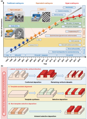 |
| The downscaling of nanomaterials, nanostructures, nanodevices and nanosystems needs atomic level deposition, and there are three characteristics of atomic level deposition including bringing lateral angstrom resolution to the vertical direction, template-assisted alignments with high accuracy, non-template selective deposition. Credit: by Rong Chen, Yi-Cheng Li, Jia-Ming Cai, Kun Cao, Han-Bo-Ram Lee |
Abstract:
Moore’s law has driven the semiconductor industry to continue downscaling the critical size of transistors to improve device density. At the beginning of this century, traditional scaling started to encounter bottlenecks. The industry has successively developed strained Si/Ge, high-K/metal gate, and Fin-FETs, enabling Moore's Law to continue. Now, the critical size of FETs is down to 7 nm, namely there’s almost 7 billion transistors per square centimeter on one chip, which brings huge challenges for fin-type structure and nanomanufacturing methods. Up to now, extreme ultraviolet lithography has been used in some critical steps, and it is facing alignment precision and high costs for high-volume manufacturing. Meanwhile, the introduction of new materials and 3D complex structures brings serious challenges for top-down methods. Newly developed bottom-up manufacturing serves as a good complementary method and provides technical driving force for nanomanufacturing. As early as 1959, Prof. Feynman speculated, “There’s plenty of room at the bottom”. This talk inspired human beings to manipulate atoms or molecules as building blocks for designed structures. Atomic level deposition is a typical representative for bottom-up strategies. In the first section, the deposition brings lateral angstrom resolution to the vertical direction as well as top-down etching, such as double patterning. Next, various template-assisted selective deposition methods including dielectric templates, inhibitors and correction steps have been utilized for the alignment of 3D complex structures. Finally, atomic scale resolution can be achieved by inherently selective deposition. Low dimensional materials and emerging applications are discussed, including 2D materials, nanowires, nanoparticles, etc. In this article, Professor Rong Chen gave a detailed introduction to the recent progresses of atomic level deposition and its potential to extend Moore’s law and beyond.
Atomic level deposition to extend Moore’s law and beyond
Wuhan, China | Posted on July 15th, 2022The atomic level deposition methods are characterized by the conformality and uniformity of thin films. Atomic level deposition can bring lateral resolution to the vertical direction for diversified structures with high aspect-ratios, including sidewalls, nanowires, nanotubes and so on. Self-aligned double patterning is a typical example for vertical resolution. Atomic level deposition can improve the accuracy of nanopatterning and obtain some special structures, which can further reduce the feature size and increase the density of transistors, thereby promoting the continuation of Moore's law in the short term.
With the devices become more complex, the aligned growth of thin films has been considered as an essential aspect during nanomanufacturing. Selective deposition is an efficient and promising method to achieve alignment, which can reduce steps such as photolithography and etching. Normally, it’s effective to achieve deposition with high selectivity by using special templates. With the help of the templates, chip makers could not only superimpose transistors directly in three dimensions, but also integrate multi-functionality, such as sensing, energy storage, into chips to manufacture super-chips.
It is quite challenging to prepare appropriate templates for selective deposition of low dimensional materials and complex 3D structures by current top-down approaches, non-template selective deposition has been studied. For the post-Si era, atomic level deposition can prepare many alternative nanomaterials, such as 2D materials, carbon materials, ferroelectric materials, phase transition materials and so on, which can overcome the constraints of the physical limits of silicon materials and broaden the boundaries of Moore's law.
Professor Chen Rong and other researchers in her group have identified a few critical challenges in the field of atomic level deposition:
“Atomic level deposition is a versatile future-oriented deposition technology, which is bound to play an increasingly important role in the field of micro-nano manufacturing. The chip makers have shown strong interest in this technology. In addition to the field of microelectronics, atomic scale deposition has a wide range of applications in optoelectronics, energy storage, catalysis, biomedicines.”
“To achieve nanomanufacturing with high precision, the mechanism of atomic level deposition needs in-depth study.”
“Although the characterization technologies are booming, the single-atom characterization and manipulation technology still have vast room for improvement.”
“To achieve complex nanostructures fabrication, multiple processes coupling is indispensable for various materials. But how to achieve process integration?”
“Besides fabricating thin films and nanostructures with high precision, accuracy and processing efficiency are inter-inhibitive factors. How to achieve reliable high-volume manufacturing in industry?”
Researchers have suggested that atomic level deposition could be used to extend Moore’s law and beyond. Atomic level deposition is becoming an increasingly promising technology for the precise fabrication of complex nanostructures, enables the creation of equivalent topography with a better control over the film thickness and without roughening the surface. It is considered as an enabling technology in advanced semiconductor technology nodes and other emerging fields.
####
For more information, please click here
Contacts:
Media Contact
Yue YAO
International Journal of Extreme Manufacturing
Expert Contact
Rong Chen
Huazhong University of Science and Technology
Copyright © International Journal of Extreme Manufacturing
If you have a comment, please Contact us.Issuers of news releases, not 7th Wave, Inc. or Nanotechnology Now, are solely responsible for the accuracy of the content.
Bookmark:


| Related News Press |
News and information
![]() Simulating magnetization in a Heisenberg quantum spin chain April 5th, 2024
Simulating magnetization in a Heisenberg quantum spin chain April 5th, 2024
![]() NRL charters Navy’s quantum inertial navigation path to reduce drift April 5th, 2024
NRL charters Navy’s quantum inertial navigation path to reduce drift April 5th, 2024
![]() Discovery points path to flash-like memory for storing qubits: Rice find could hasten development of nonvolatile quantum memory April 5th, 2024
Discovery points path to flash-like memory for storing qubits: Rice find could hasten development of nonvolatile quantum memory April 5th, 2024
Possible Futures
![]() Discovery points path to flash-like memory for storing qubits: Rice find could hasten development of nonvolatile quantum memory April 5th, 2024
Discovery points path to flash-like memory for storing qubits: Rice find could hasten development of nonvolatile quantum memory April 5th, 2024
![]() With VECSELs towards the quantum internet Fraunhofer: IAF achieves record output power with VECSEL for quantum frequency converters April 5th, 2024
With VECSELs towards the quantum internet Fraunhofer: IAF achieves record output power with VECSEL for quantum frequency converters April 5th, 2024
Chip Technology
![]() Discovery points path to flash-like memory for storing qubits: Rice find could hasten development of nonvolatile quantum memory April 5th, 2024
Discovery points path to flash-like memory for storing qubits: Rice find could hasten development of nonvolatile quantum memory April 5th, 2024
![]() Utilizing palladium for addressing contact issues of buried oxide thin film transistors April 5th, 2024
Utilizing palladium for addressing contact issues of buried oxide thin film transistors April 5th, 2024
![]() HKUST researchers develop new integration technique for efficient coupling of III-V and silicon February 16th, 2024
HKUST researchers develop new integration technique for efficient coupling of III-V and silicon February 16th, 2024
Nanoelectronics
![]() Interdisciplinary: Rice team tackles the future of semiconductors Multiferroics could be the key to ultralow-energy computing October 6th, 2023
Interdisciplinary: Rice team tackles the future of semiconductors Multiferroics could be the key to ultralow-energy computing October 6th, 2023
![]() Key element for a scalable quantum computer: Physicists from Forschungszentrum Jülich and RWTH Aachen University demonstrate electron transport on a quantum chip September 23rd, 2022
Key element for a scalable quantum computer: Physicists from Forschungszentrum Jülich and RWTH Aachen University demonstrate electron transport on a quantum chip September 23rd, 2022
![]() Reduced power consumption in semiconductor devices September 23rd, 2022
Reduced power consumption in semiconductor devices September 23rd, 2022
![]() Controlled synthesis of crystal flakes paves path for advanced future electronics June 17th, 2022
Controlled synthesis of crystal flakes paves path for advanced future electronics June 17th, 2022
Discoveries
![]() Chemical reactions can scramble quantum information as well as black holes April 5th, 2024
Chemical reactions can scramble quantum information as well as black holes April 5th, 2024
![]() New micromaterial releases nanoparticles that selectively destroy cancer cells April 5th, 2024
New micromaterial releases nanoparticles that selectively destroy cancer cells April 5th, 2024
![]() Utilizing palladium for addressing contact issues of buried oxide thin film transistors April 5th, 2024
Utilizing palladium for addressing contact issues of buried oxide thin film transistors April 5th, 2024
Announcements
![]() NRL charters Navy’s quantum inertial navigation path to reduce drift April 5th, 2024
NRL charters Navy’s quantum inertial navigation path to reduce drift April 5th, 2024
![]() Discovery points path to flash-like memory for storing qubits: Rice find could hasten development of nonvolatile quantum memory April 5th, 2024
Discovery points path to flash-like memory for storing qubits: Rice find could hasten development of nonvolatile quantum memory April 5th, 2024
Interviews/Book Reviews/Essays/Reports/Podcasts/Journals/White papers/Posters
![]() Simulating magnetization in a Heisenberg quantum spin chain April 5th, 2024
Simulating magnetization in a Heisenberg quantum spin chain April 5th, 2024
![]() Discovery points path to flash-like memory for storing qubits: Rice find could hasten development of nonvolatile quantum memory April 5th, 2024
Discovery points path to flash-like memory for storing qubits: Rice find could hasten development of nonvolatile quantum memory April 5th, 2024
Tools
![]() Ferroelectrically modulate the Fermi level of graphene oxide to enhance SERS response November 3rd, 2023
Ferroelectrically modulate the Fermi level of graphene oxide to enhance SERS response November 3rd, 2023
![]() The USTC realizes In situ electron paramagnetic resonance spectroscopy using single nanodiamond sensors November 3rd, 2023
The USTC realizes In situ electron paramagnetic resonance spectroscopy using single nanodiamond sensors November 3rd, 2023
|
|
||
|
|
||
| The latest news from around the world, FREE | ||
|
|
||
|
|
||
| Premium Products | ||
|
|
||
|
Only the news you want to read!
Learn More |
||
|
|
||
|
Full-service, expert consulting
Learn More |
||
|
|
||