Home > Press > Getting electrons to move in a semiconductor: Gallium oxide shows high electron mobility, making it promising for better and cheaper devices
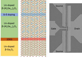 |
| Schematic stack and the scanning electron microscopic image of the β-(AlxGa1-x)2O3/Ga2O3 modulation-doped field effect transistor. CREDIT Choong Hee Lee and Yuewei Zhang |
Abstract:
The next generation of energy-efficient power electronics, high-frequency communication systems, and solid-state lighting rely on materials known as wide bandgap semiconductors. Circuits based on these materials can operate at much higher power densities and with lower power losses than silicon-based circuits. These materials have enabled a revolution in LED lighting, which led to the 2014 Nobel Prize in physics.
Getting electrons to move in a semiconductor: Gallium oxide shows high electron mobility, making it promising for better and cheaper devices
Washington, DC | Posted on April 24th, 2018In new experiments reported in Applied Physics Letters, from AIP Publishing, researchers have shown that a wide-bandgap semiconductor called gallium oxide (Ga2O3) can be engineered into nanometer-scale structures that allow electrons to move much faster within the crystal structure. With electrons that move with such ease, Ga2O3 could be a promising material for applications such as high-frequency communication systems and energy-efficient power electronics.
"Gallium oxide has the potential to enable transistors that would surpass current technology," said Siddharth Rajan of Ohio State University, who led the research.
Because Ga2O3 has one of the largest bandgaps (the energy needed to excite an electron so that it's conductive) of the wide bandgap materials being developed as alternatives to silicon, it's especially useful for high-power and high-frequency devices. It's also unique among wide bandgap semiconductors in that it can be produced directly from its molten form, which enables large-scale manufacturing of high-quality crystals.
For use in electronic devices, the electrons in the material must be able to move easily under an electric field, a property called high electron mobility. "That's a key parameter for any device," Rajan said. Normally, to populate a semiconductor with electrons, the material is doped with other elements. The problem, however, is that the dopants also scatter electrons, limiting the electron mobility of the material.
To solve this problem, the researchers used a technique known as modulation doping. The approach was first developed in 1979 by Takashi Mimura to create a gallium arsenide high-electron mobility transistor, which won the Kyoto Prize in 2017. While it is now a commonly used technique to achieve high mobility, its application to Ga2O3 is something new.
In their work, the researchers created a so-called semiconductor heterostructure, creating an atomically perfect interface between Ga2O3 and its alloy with aluminum, aluminum gallium oxide -- two semiconductors with the same crystal structure but different energy gaps. A few nanometers away from the interface, embedded inside the aluminum gallium oxide, is a sheet of electron-donating impurities only a few atoms thick. The donated electrons transfer into the Ga2O3, forming a 2-D electron gas. But because the electrons are now also separated from the dopants (hence the term modulation doping) in the aluminum gallium oxide by a few nanometers, they scatter much less and remain highly mobile.
Using this technique, the researchers reached record mobilities. The researchers were also able to observe Shubnikov-de Haas oscillations, a quantum phenomenon in which increasing the strength of an external magnetic field causes the resistance of the material to oscillate. These oscillations confirm formation of the high mobility 2-D electron gas and allow the researchers to measure critical material properties.
Rajan explained that such modulation-doped structures could lead to a new class of quantum structures and electronics that harnesses the potential of Ga2O3.
####
About American Institute of Physics
Applied Physics Letters features concise, rapid reports on significant new findings in applied physics. The journal covers new experimental and theoretical research on applications of physics phenomena related to all branches of science, engineering, and modern technology. See http://apl.aip.org .
For more information, please click here
Contacts:
Julia Majors
301-209-3090
Copyright © American Institute of Physics
If you have a comment, please Contact us.Issuers of news releases, not 7th Wave, Inc. or Nanotechnology Now, are solely responsible for the accuracy of the content.
Bookmark:


| Related Links |
| Related News Press |
News and information
![]() Researchers develop molecular qubits that communicate at telecom frequencies October 3rd, 2025
Researchers develop molecular qubits that communicate at telecom frequencies October 3rd, 2025
![]() Next-generation quantum communication October 3rd, 2025
Next-generation quantum communication October 3rd, 2025
![]() "Nanoreactor" cage uses visible light for catalytic and ultra-selective cross-cycloadditions October 3rd, 2025
"Nanoreactor" cage uses visible light for catalytic and ultra-selective cross-cycloadditions October 3rd, 2025
Display technology/LEDs/SS Lighting/OLEDs
![]() Spinel-type sulfide semiconductors to operate the next-generation LEDs and solar cells For solar-cell absorbers and green-LED source October 3rd, 2025
Spinel-type sulfide semiconductors to operate the next-generation LEDs and solar cells For solar-cell absorbers and green-LED source October 3rd, 2025
2 Dimensional Materials
![]() ICFO researchers overcome long-standing bottleneck in single photon detection with twisted 2D materials August 8th, 2025
ICFO researchers overcome long-standing bottleneck in single photon detection with twisted 2D materials August 8th, 2025
![]() First real-time observation of two-dimensional melting process: Researchers at Mainz University unveil new insights into magnetic vortex structures August 8th, 2025
First real-time observation of two-dimensional melting process: Researchers at Mainz University unveil new insights into magnetic vortex structures August 8th, 2025
![]() Lab to industry: InSe wafer-scale breakthrough for future electronics August 8th, 2025
Lab to industry: InSe wafer-scale breakthrough for future electronics August 8th, 2025
Hardware
![]() The present and future of computing get a boost from new research July 21st, 2023
The present and future of computing get a boost from new research July 21st, 2023
![]() A Carbon Nanotube Microprocessor Mature Enough to Say Hello: Three new breakthroughs make commercial nanotube processors possible March 2nd, 2020
A Carbon Nanotube Microprocessor Mature Enough to Say Hello: Three new breakthroughs make commercial nanotube processors possible March 2nd, 2020
![]() Powering the future: Smallest all-digital circuit opens doors to 5 nm next-gen semiconductor February 11th, 2020
Powering the future: Smallest all-digital circuit opens doors to 5 nm next-gen semiconductor February 11th, 2020
Possible Futures
![]() Spinel-type sulfide semiconductors to operate the next-generation LEDs and solar cells For solar-cell absorbers and green-LED source October 3rd, 2025
Spinel-type sulfide semiconductors to operate the next-generation LEDs and solar cells For solar-cell absorbers and green-LED source October 3rd, 2025
Chip Technology
![]() Lab to industry: InSe wafer-scale breakthrough for future electronics August 8th, 2025
Lab to industry: InSe wafer-scale breakthrough for future electronics August 8th, 2025
![]() A 1960s idea inspires NBI researchers to study hitherto inaccessible quantum states June 6th, 2025
A 1960s idea inspires NBI researchers to study hitherto inaccessible quantum states June 6th, 2025
![]() Programmable electron-induced color router array May 14th, 2025
Programmable electron-induced color router array May 14th, 2025
Nanoelectronics
![]() Lab to industry: InSe wafer-scale breakthrough for future electronics August 8th, 2025
Lab to industry: InSe wafer-scale breakthrough for future electronics August 8th, 2025
![]() Interdisciplinary: Rice team tackles the future of semiconductors Multiferroics could be the key to ultralow-energy computing October 6th, 2023
Interdisciplinary: Rice team tackles the future of semiconductors Multiferroics could be the key to ultralow-energy computing October 6th, 2023
![]() Key element for a scalable quantum computer: Physicists from Forschungszentrum J�lich and RWTH Aachen University demonstrate electron transport on a quantum chip September 23rd, 2022
Key element for a scalable quantum computer: Physicists from Forschungszentrum J�lich and RWTH Aachen University demonstrate electron transport on a quantum chip September 23rd, 2022
![]() Reduced power consumption in semiconductor devices September 23rd, 2022
Reduced power consumption in semiconductor devices September 23rd, 2022
Discoveries
![]() Researchers develop molecular qubits that communicate at telecom frequencies October 3rd, 2025
Researchers develop molecular qubits that communicate at telecom frequencies October 3rd, 2025
![]() Next-generation quantum communication October 3rd, 2025
Next-generation quantum communication October 3rd, 2025
![]() "Nanoreactor" cage uses visible light for catalytic and ultra-selective cross-cycloadditions October 3rd, 2025
"Nanoreactor" cage uses visible light for catalytic and ultra-selective cross-cycloadditions October 3rd, 2025
Materials/Metamaterials/Magnetoresistance
![]() First real-time observation of two-dimensional melting process: Researchers at Mainz University unveil new insights into magnetic vortex structures August 8th, 2025
First real-time observation of two-dimensional melting process: Researchers at Mainz University unveil new insights into magnetic vortex structures August 8th, 2025
![]() Researchers unveil a groundbreaking clay-based solution to capture carbon dioxide and combat climate change June 6th, 2025
Researchers unveil a groundbreaking clay-based solution to capture carbon dioxide and combat climate change June 6th, 2025
![]() A 1960s idea inspires NBI researchers to study hitherto inaccessible quantum states June 6th, 2025
A 1960s idea inspires NBI researchers to study hitherto inaccessible quantum states June 6th, 2025
![]() Institute for Nanoscience hosts annual proposal planning meeting May 16th, 2025
Institute for Nanoscience hosts annual proposal planning meeting May 16th, 2025
Announcements
![]() Rice membrane extracts lithium from brines with greater speed, less waste October 3rd, 2025
Rice membrane extracts lithium from brines with greater speed, less waste October 3rd, 2025
![]() Researchers develop molecular qubits that communicate at telecom frequencies October 3rd, 2025
Researchers develop molecular qubits that communicate at telecom frequencies October 3rd, 2025
![]() Next-generation quantum communication October 3rd, 2025
Next-generation quantum communication October 3rd, 2025
![]() "Nanoreactor" cage uses visible light for catalytic and ultra-selective cross-cycloadditions October 3rd, 2025
"Nanoreactor" cage uses visible light for catalytic and ultra-selective cross-cycloadditions October 3rd, 2025
Interviews/Book Reviews/Essays/Reports/Podcasts/Journals/White papers/Posters
![]() Spinel-type sulfide semiconductors to operate the next-generation LEDs and solar cells For solar-cell absorbers and green-LED source October 3rd, 2025
Spinel-type sulfide semiconductors to operate the next-generation LEDs and solar cells For solar-cell absorbers and green-LED source October 3rd, 2025
![]() Rice membrane extracts lithium from brines with greater speed, less waste October 3rd, 2025
Rice membrane extracts lithium from brines with greater speed, less waste October 3rd, 2025
Grants/Sponsored Research/Awards/Scholarships/Gifts/Contests/Honors/Records
![]() Researchers tackle the memory bottleneck stalling quantum computing October 3rd, 2025
Researchers tackle the memory bottleneck stalling quantum computing October 3rd, 2025
![]() New discovery aims to improve the design of microelectronic devices September 13th, 2024
New discovery aims to improve the design of microelectronic devices September 13th, 2024
![]() Physicists unlock the secret of elusive quantum negative entanglement entropy using simple classical hardware August 16th, 2024
Physicists unlock the secret of elusive quantum negative entanglement entropy using simple classical hardware August 16th, 2024
|
|
||
|
|
||
| The latest news from around the world, FREE | ||
|
|
||
|
|
||
| Premium Products | ||
|
|
||
|
Only the news you want to read!
Learn More |
||
|
|
||
|
Full-service, expert consulting
Learn More |
||
|
|
||