Home > Press > Miracle Material: Two-dimensional graphene may lead to faster electronics, stronger spacecraft and much more
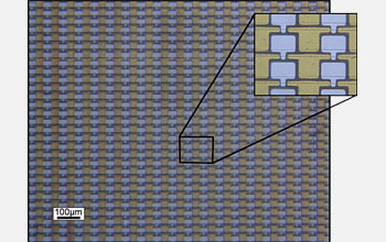 |
| Optical micrograph of an array of graphene transistors prepared on silicon carbide (SiC). There are 40,000 devices per square centimeter.
Credit: M. Sprinkle, M. Ruan,Y. Hu, J. Hankinson,M. Rubio-Roy, B. Zhang, X. Wu, C. Berger & W. A. de Heer. (2010). Scalable templated growth of graphene nanoribbons on SiC. Nature Nanotechnology (5), 727-731. |
Abstract:
In the 19th century novel, Flatland, by Edward A. Abbott, residents of that fictional country exist in only two dimensions. Women are born as line segments, while men come in a range of geometric shapes reflecting their rank, from lowly isosceles triangles, to middle-class squares, to six-sided hexagons, reserved for nobility.
Miracle Material: Two-dimensional graphene may lead to faster electronics, stronger spacecraft and much more
Arlington, VA | Posted on May 19th, 2011The constraints of life on a flat plane satirically reflect the rigid Victorian class structure of Abbott's time. When the narrator of the story discovers a third dimension, height, he tries to communicate this freeing concept to fellow Flatlanders, and winds up in jail.
Graphene, a real-life version of Flatland, consists of row upon row of hexagonal rings of carbon atoms fitted together in a flat honeycomb pattern only a single atom thick.
This atomic scale makes graphene part of the nano-world, where objects a thousand times thinner than a human hair no longer follow familiar natural laws such as friction and gravity.
Just as the narrator of Flatland rises above his restricted existence to experience life in another dimension, objects on the nano-scale obey a new set of rules: the "spooky" laws of quantum mechanics.
Quantum quirks
One of the most exciting quantum mechanical effects in graphene is the high speed at which electrons can flow through it due to a lack of friction. This so-called "ballistic" transport could lead to a new generation of superfast, super-efficient electronics.
In addition, for its size, graphene is stronger and more flexible than steel. It conducts heat 10 times faster than copper and can carry 1,000 times the density of electric current as copper wires.
In fact, graphene's structure gives it many unique optical, thermal, mechanical and electrical properties, exciting engineers and scientists all over the world with grand new possibilities for all sorts of applications.
Growing graphene
Graphene was discovered by early 20th-century scientists looking at common graphite using X-ray spectroscopy. Although they could tell that the graphite was composed of a stack of individual graphene layers, no one saw any use for these ultrathin layers at the time.
In the 1990s, scientists learned how to make carbon nanotubes (CNTs), which are tiny, rolled-up tubes of carbon atoms arranged in the same hexagonal chicken wire pattern as graphene.
It wasn't until 2004 that scientists measured the electronic properties of thin layers of graphene after teasing apart flakes of graphite pencil lead using transparent tape. But this tedious method of creating graphene would never work for a commercially viable product.
Surpassing silicon
Meanwhile, Georgia Tech scientists Walter de Heer, Claire Berger (also affiliated with CNRS, France) and Phillip First had been working with CNTs. They hoped to use the nano-scale tubes to speed up the next generation of microelectronic components that would exceed the capacity of silicon electronics.
But even though CNTs had ballistic electron transport speed, they were hard to assemble into integrated circuits.
In 2001, de Heer thought that perhaps two-dimensional graphene could be used as an electronic material also, since it is the basis of carbon nanotubes. That year, he submitted a research proposal to the National Science Foundation (NSF) for a grant to study the use of graphene in electronics.
De Heer and his team came up with the idea of growing a flat layer of graphene right where it would be used on a chip, and in the exact size and shape needed, so that it could be pre-integrated into an electrical device. This would be much easier than producing the delicate CNTs, transferring them to another spot, and then connecting them with a metal wire to a circuit.
First graphene patent
In 2003, the Georgia Tech team was the first to file a patent for a process of making simple electronic devices using graphene produced epitaxially (epitaxial means growing a layer of one substance on top of another material so both materials have the same structural orientation).
The team's basic method was to heat a crystalline wafer of silicon carbide (SiC) to high temperatures (greater than 1100 C). At that temperature, the silicon atoms evaporated off the surface leaving only carbon atoms, which rearranged themselves into graphene's familiar chicken-wire pattern.
Epitaxial graphene can be grown on top of different supporting materials, depending on what it's to be used for. One huge advantage of epitaxial graphene is that it uses the same kinds of chemical processes that developers already use to make silicon-based electronics.
"It's more than just having the graphene material," de Heer said. "It's actually having the platform and processing techniques that would be developed in parallel."
Since their initial proposal, de Heer and his team, funded by NSF through the Georgia Tech Materials Research Science and Engineering Center (MRSEC), have gone on to receive other patents and publish dozens of research papers on epitaxial graphene for electronics. In 2010, de Heer was awarded the MRS Medal from the Materials Research Society for his pioneering contributions to the science and technology of epitaxial graphene.
Graphene makes it stronger
Graphene's superior electronic properties aren't its only strong suit. Nikhil Koratkar, professor of mechanical, aerospace and nuclear engineering at Rensselaer Polytechnic Institute, is using sheets of graphene to strengthen ceramic composites for tough environments like outer space.
"I am very interested in developing practical applications of nano-materials, such as graphene and carbon nanotubes," said Koratkar. "Nano-composites are one such application which can have strong impact."
Koratkar is working with Erica L. Corral, assistant professor at the University of Arizona's department of materials science and engineering, and a specialist in ceramic composites.
Before Koratkar and Corral teamed up, graphene had been used in polymer composites but never in ceramics for improving its mechanical strength. Ceramics are among the most high-temperature resistant materials in the world, but they tend to be very brittle.
Preventing cracks
In the search for something to add to ceramic composites that would prevent cracking, the scientists chose graphene for its mechanical strength, surface area and geometry. "Graphene shows remarkable stiffness and strength," Koratkar said. "And even though it is only nanometers thick, it comes in sheets large enough to wrap and anchor itself securely around ceramic grains during the sintering process used to manufacture ceramics."
The results of Koratkar and Corral's research were encouraging. "We have shown that graphene can toughen silicon nitride ceramics by greater than 200 percent," he said. "The reason for this toughening is that the two-dimensional graphene sheets are able to deflect propagating cracks in not just two but in three dimensions."
Koratkar and Corral, supported by grants from NSF, will continue to explore the use of graphene in other types of ceramics and study the performance of the composite with higher percentages of graphene.
"The future of graphene in ceramics should result in a new field of materials research and composite systems that is far more advanced than the one-dimensional reinforcement systems we have used to date," said Corral.
Graphing the graphene industry
With so much graphene research going on in a multitude of industries, it's hard to keep track. But Jan Youtie, a social scientist and principal research associate at Georgia Tech's Enterprise Innovation Institute, along with her colleague Philip Shapira, professor at Georgia Tech's School of Public Policy and the University of Manchester, are doing just that.
The researchers use a process called "real-time technology assessment" (RTTA) to understand the social, moral, political and economic dynamics of the nanotechnology industry, including graphene. To do this, they collect all patent applications and every scientific paper covering graphene into a database.
"Graphene has experienced a steep trajectory in terms of research output and discoveries," Youtie said. "This trajectory is even earlier and steeper than we have seen with respect to other nanotechnologies."
Youtie and Shapira's research is funded by NSF through the Center for Nanotechnology in Society at Arizona State University (CNS-ASU), which unifies research programs across several universities. They have discovered that Atlanta, where Georgia Tech is located, is one of the leading nodes of graphene research in the world, based on total number of publications.
Global graphene
"There are nearly 200 companies, including large multinational corporations and small startup firms that have become involved in the graphene domain," Youtie said. "This means that new applications are being considered while the research is still being conducted."
Just in the past year, Youtie has recorded patents using graphene in an alcohol fuel battery, Bakelite� powder filler, organic single crystal transistors, controlled drug release systems, dye-sensitized solar cells, wastewater dyeing, thin film composites/conductive composites/polymer composites/plastic-wood composites, water resistant fiber board, metallic foam, battery cathode material, printing and a proton exchange membrane fuel battery.
"There is global participation in graphene research and commercialization, and the top companies are large corporations from Korea and Japan, with U.S. companies present but not as prevalent," Youtie said. "The internationalization in this domain reflects the transcendence of nanotechnology in general across national borders."
-- Holly B. Martin
Investigators
Dennis Hess
Catalin Picu
David Guston
Erica Corral
Walter De Heer
Nikhil Koratkar
Related Institutions/Organizations
Arizona State University
Georgia Tech Research Corporation
Rensselaer Polytechnic Institute
University of Arizona
Locations
Arizona
Georgia
New York
####
For more information, please click here
Contacts:
The National Science Foundation
4201 Wilson Boulevard
Arlington, Virginia 22230, USA
Tel: (703) 292-5111
FIRS: (800) 877-8339
TDD: (800) 281-8749
Copyright © National Science Foundation
If you have a comment, please Contact us.Issuers of news releases, not 7th Wave, Inc. or Nanotechnology Now, are solely responsible for the accuracy of the content.
Bookmark:


| Related News Press |
News and information
![]() Simulating magnetization in a Heisenberg quantum spin chain April 5th, 2024
Simulating magnetization in a Heisenberg quantum spin chain April 5th, 2024
![]() NRL charters Navy�s quantum inertial navigation path to reduce drift April 5th, 2024
NRL charters Navy�s quantum inertial navigation path to reduce drift April 5th, 2024
![]() Discovery points path to flash-like memory for storing qubits: Rice find could hasten development of nonvolatile quantum memory April 5th, 2024
Discovery points path to flash-like memory for storing qubits: Rice find could hasten development of nonvolatile quantum memory April 5th, 2024
Graphene/ Graphite
![]() NRL discovers two-dimensional waveguides February 16th, 2024
NRL discovers two-dimensional waveguides February 16th, 2024
Govt.-Legislation/Regulation/Funding/Policy
![]() NRL charters Navy�s quantum inertial navigation path to reduce drift April 5th, 2024
NRL charters Navy�s quantum inertial navigation path to reduce drift April 5th, 2024
![]() Discovery points path to flash-like memory for storing qubits: Rice find could hasten development of nonvolatile quantum memory April 5th, 2024
Discovery points path to flash-like memory for storing qubits: Rice find could hasten development of nonvolatile quantum memory April 5th, 2024
![]() Chemical reactions can scramble quantum information as well as black holes April 5th, 2024
Chemical reactions can scramble quantum information as well as black holes April 5th, 2024
Chip Technology
![]() Discovery points path to flash-like memory for storing qubits: Rice find could hasten development of nonvolatile quantum memory April 5th, 2024
Discovery points path to flash-like memory for storing qubits: Rice find could hasten development of nonvolatile quantum memory April 5th, 2024
![]() Utilizing palladium for addressing contact issues of buried oxide thin film transistors April 5th, 2024
Utilizing palladium for addressing contact issues of buried oxide thin film transistors April 5th, 2024
![]() HKUST researchers develop new integration technique for efficient coupling of III-V and silicon February 16th, 2024
HKUST researchers develop new integration technique for efficient coupling of III-V and silicon February 16th, 2024
Nanoelectronics
![]() Interdisciplinary: Rice team tackles the future of semiconductors Multiferroics could be the key to ultralow-energy computing October 6th, 2023
Interdisciplinary: Rice team tackles the future of semiconductors Multiferroics could be the key to ultralow-energy computing October 6th, 2023
![]() Key element for a scalable quantum computer: Physicists from Forschungszentrum J�lich and RWTH Aachen University demonstrate electron transport on a quantum chip September 23rd, 2022
Key element for a scalable quantum computer: Physicists from Forschungszentrum J�lich and RWTH Aachen University demonstrate electron transport on a quantum chip September 23rd, 2022
![]() Reduced power consumption in semiconductor devices September 23rd, 2022
Reduced power consumption in semiconductor devices September 23rd, 2022
![]() Atomic level deposition to extend Moore�s law and beyond July 15th, 2022
Atomic level deposition to extend Moore�s law and beyond July 15th, 2022
Discoveries
![]() Chemical reactions can scramble quantum information as well as black holes April 5th, 2024
Chemical reactions can scramble quantum information as well as black holes April 5th, 2024
![]() New micromaterial releases nanoparticles that selectively destroy cancer cells April 5th, 2024
New micromaterial releases nanoparticles that selectively destroy cancer cells April 5th, 2024
![]() Utilizing palladium for addressing contact issues of buried oxide thin film transistors April 5th, 2024
Utilizing palladium for addressing contact issues of buried oxide thin film transistors April 5th, 2024
Materials/Metamaterials/Magnetoresistance
![]() Nanoscale CL thermometry with lanthanide-doped heavy-metal oxide in TEM March 8th, 2024
Nanoscale CL thermometry with lanthanide-doped heavy-metal oxide in TEM March 8th, 2024
![]() Focused ion beam technology: A single tool for a wide range of applications January 12th, 2024
Focused ion beam technology: A single tool for a wide range of applications January 12th, 2024
Announcements
![]() NRL charters Navy�s quantum inertial navigation path to reduce drift April 5th, 2024
NRL charters Navy�s quantum inertial navigation path to reduce drift April 5th, 2024
![]() Discovery points path to flash-like memory for storing qubits: Rice find could hasten development of nonvolatile quantum memory April 5th, 2024
Discovery points path to flash-like memory for storing qubits: Rice find could hasten development of nonvolatile quantum memory April 5th, 2024
Patents/IP/Tech Transfer/Licensing
![]() Getting drugs across the blood-brain barrier using nanoparticles March 3rd, 2023
Getting drugs across the blood-brain barrier using nanoparticles March 3rd, 2023
![]() Metasurfaces control polarized light at will: New research unlocks the hidden potential of metasurfaces August 13th, 2021
Metasurfaces control polarized light at will: New research unlocks the hidden potential of metasurfaces August 13th, 2021
![]() Arrowhead Pharmaceuticals Announces Closing of Agreement with Takeda November 27th, 2020
Arrowhead Pharmaceuticals Announces Closing of Agreement with Takeda November 27th, 2020
Aerospace/Space
![]() Under pressure - space exploration in our time: Advancing space exploration through diverse collaborations and ethical policies February 16th, 2024
Under pressure - space exploration in our time: Advancing space exploration through diverse collaborations and ethical policies February 16th, 2024
![]() Bridging light and electrons January 12th, 2024
Bridging light and electrons January 12th, 2024
![]() Manufacturing advances bring material back in vogue January 20th, 2023
Manufacturing advances bring material back in vogue January 20th, 2023
|
|
||
|
|
||
| The latest news from around the world, FREE | ||
|
|
||
|
|
||
| Premium Products | ||
|
|
||
|
Only the news you want to read!
Learn More |
||
|
|
||
|
Full-service, expert consulting
Learn More |
||
|
|
||