Home > Press > Stressed Nanomaterials Display Unexpected Movement
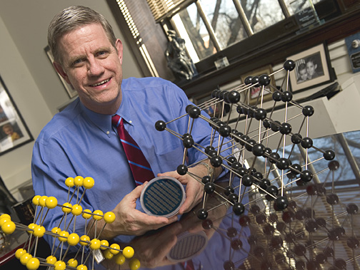 |
| Kevin Hemker, seated between models representing how atoms are packed within an individual grain in a material, holds a silicon wafer onto which nanocrystalline aluminum thin film specimens have been deposited. Photo: Will Kirk/Homewoodphoto.jhu.edu |
Abstract:
Johns Hopkins researchers have discovered that, under the right conditions, newly developed nanocrystalline materials exhibit surprising activity in the tiny spaces between the geometric clusters of atoms called nanocrystals, from which they are made.
Stressed Nanomaterials Display Unexpected Movement
Baltimore, MD | Posted on March 1st, 2010This finding, detailed recently in the journal Science, is important because these nanomaterials are becoming more ubiquitous in the fabrication of microdevices and integrated circuits. Movement in the atomic realm can affect the mechanical properties of these futuristic materials�making them more flexible and less brittle�and may alter the material's lifespan.
"As we make smaller and smaller devices, we've been using more nanocrystalline materials that have much smaller crystallites�what materials scientists call grains�and are believed to be much stronger," said Kevin Hemker, professor and chair of Mechanical Engineering in Johns Hopkins' Whiting School of Engineering and senior author of the Science article. "But we have to understand more about how these new types of metal and ceramic components behave, compared to traditional materials. How do we predict their reliability? How might these materials deform when they are subjected to stress?"
The experiments conducted by a former undergraduate research assistant and supervised by Hemker focused on what happens in regions called grain boundaries. A grain or crystallite is a tiny cluster of atoms arranged in an orderly three-dimensional pattern. The irregular space or interface between two grains with different geometric orientations is called the grain boundary. Grain boundaries can contribute to a material's strength and help it resist plastic deformation, a permanent change of shape. Nanomaterials are believed to be stronger than traditional metals and ceramics because they possess smaller grains and, as a result, have more grain boundaries.
Most scientists have been taught that these grain boundaries do not move, a characteristic that helps the material resist deformation. But when Hemker and his colleagues performed experiments on nanocrystalline aluminum thin films, applying a type of force called shear stress, they found an unexpected result. "We saw that the grains had grown bigger, which can only occur if the boundaries move," he said, "and the most surprising part of our observation was that it was shear stress that had caused the boundaries to move."
"The original view," Hemker said, "was that these boundaries were like the walls inside of a house. The walls and the rooms they create don't change size; the only activity is by people moving around inside the room. But our experiments showed that in these nanomaterials, when you apply a particular type of force, the rooms do change size because the walls actually move."
The discovery has implications for those who use thin films and other nanomaterials to make integrated circuits and microelectromechanical systems, commonly called MEMS. The boundary movement shown by Hemker and his colleagues means that the nanomaterials used in these products likely possess more plasticity, higher reliability and less brittleness, but also reduced strength.
"As we move toward making things at much smaller sizes, we need to take into account how activity at the atomic level affects the mechanical properties of the material," Hemker said. "This knowledge can help the microdevice makers decide on the proper size for their components and can lead to better predictions about how long their products will last."
The journal article describing this discovery was inspired by a Johns Hopkins master's thesis produced by Tim Rupert, then a combined bachelor's/master's degree student in mechanical engineering. Rupert, who is now a doctoral student at MIT, is lead author of the Science piece. Along with Hemker, the co-authors are Daniel Gianola, a former doctoral student and postdoctoral fellow in Hemker's lab who is now an assistant professor of materials science and engineering at the University of Pennsylvania; and Y. Gan of the Karlsruhe Institute of Technology in Germany.
Funding for the research was provided by the U.S. Department of Energy and the National Science Foundation.
Related links:
Kevin Hemker's Lab Page: www.me.jhu.edu/hemker/MicroNano/index.html
Johns Hopkins Department of Mechanical Engineering: www.me.jhu.edu/
####
About Johns Hopkins University
The mission of The Johns Hopkins University is to educate its students and cultivate their capacity for life-long learning, to foster independent and original research, and to bring the benefits of discovery to the world.
For more information, please click here
Contacts:
MEDIA CONTACT:
Phil Sneiderman
443-287-9960
Copyright © Johns Hopkins University
If you have a comment, please Contact us.Issuers of news releases, not 7th Wave, Inc. or Nanotechnology Now, are solely responsible for the accuracy of the content.
Bookmark:


| Related News Press |
News and information
![]() Simulating magnetization in a Heisenberg quantum spin chain April 5th, 2024
Simulating magnetization in a Heisenberg quantum spin chain April 5th, 2024
![]() NRL charters Navy�s quantum inertial navigation path to reduce drift April 5th, 2024
NRL charters Navy�s quantum inertial navigation path to reduce drift April 5th, 2024
![]() Discovery points path to flash-like memory for storing qubits: Rice find could hasten development of nonvolatile quantum memory April 5th, 2024
Discovery points path to flash-like memory for storing qubits: Rice find could hasten development of nonvolatile quantum memory April 5th, 2024
![]() Good as gold - improving infectious disease testing with gold nanoparticles April 5th, 2024
Good as gold - improving infectious disease testing with gold nanoparticles April 5th, 2024
Thin films
![]() Utilizing palladium for addressing contact issues of buried oxide thin film transistors April 5th, 2024
Utilizing palladium for addressing contact issues of buried oxide thin film transistors April 5th, 2024
![]() Understanding the mechanism of non-uniform formation of diamond film on tools: Paving the way to a dry process with less environmental impact March 24th, 2023
Understanding the mechanism of non-uniform formation of diamond film on tools: Paving the way to a dry process with less environmental impact March 24th, 2023
![]() New study introduces the best graphite films: The work by Distinguished Professor Feng Ding at UNIST has been published in the October 2022 issue of Nature Nanotechnology November 4th, 2022
New study introduces the best graphite films: The work by Distinguished Professor Feng Ding at UNIST has been published in the October 2022 issue of Nature Nanotechnology November 4th, 2022
Govt.-Legislation/Regulation/Funding/Policy
![]() NRL charters Navy�s quantum inertial navigation path to reduce drift April 5th, 2024
NRL charters Navy�s quantum inertial navigation path to reduce drift April 5th, 2024
![]() Discovery points path to flash-like memory for storing qubits: Rice find could hasten development of nonvolatile quantum memory April 5th, 2024
Discovery points path to flash-like memory for storing qubits: Rice find could hasten development of nonvolatile quantum memory April 5th, 2024
![]() Chemical reactions can scramble quantum information as well as black holes April 5th, 2024
Chemical reactions can scramble quantum information as well as black holes April 5th, 2024
Possible Futures
![]() Discovery points path to flash-like memory for storing qubits: Rice find could hasten development of nonvolatile quantum memory April 5th, 2024
Discovery points path to flash-like memory for storing qubits: Rice find could hasten development of nonvolatile quantum memory April 5th, 2024
![]() With VECSELs towards the quantum internet Fraunhofer: IAF achieves record output power with VECSEL for quantum frequency converters April 5th, 2024
With VECSELs towards the quantum internet Fraunhofer: IAF achieves record output power with VECSEL for quantum frequency converters April 5th, 2024
Academic/Education
![]() Rice University launches Rice Synthetic Biology Institute to improve lives January 12th, 2024
Rice University launches Rice Synthetic Biology Institute to improve lives January 12th, 2024
![]() Multi-institution, $4.6 million NSF grant to fund nanotechnology training September 9th, 2022
Multi-institution, $4.6 million NSF grant to fund nanotechnology training September 9th, 2022
MEMS
Nanoelectronics
![]() Interdisciplinary: Rice team tackles the future of semiconductors Multiferroics could be the key to ultralow-energy computing October 6th, 2023
Interdisciplinary: Rice team tackles the future of semiconductors Multiferroics could be the key to ultralow-energy computing October 6th, 2023
![]() Key element for a scalable quantum computer: Physicists from Forschungszentrum J�lich and RWTH Aachen University demonstrate electron transport on a quantum chip September 23rd, 2022
Key element for a scalable quantum computer: Physicists from Forschungszentrum J�lich and RWTH Aachen University demonstrate electron transport on a quantum chip September 23rd, 2022
![]() Reduced power consumption in semiconductor devices September 23rd, 2022
Reduced power consumption in semiconductor devices September 23rd, 2022
![]() Atomic level deposition to extend Moore�s law and beyond July 15th, 2022
Atomic level deposition to extend Moore�s law and beyond July 15th, 2022
Discoveries
![]() Chemical reactions can scramble quantum information as well as black holes April 5th, 2024
Chemical reactions can scramble quantum information as well as black holes April 5th, 2024
![]() New micromaterial releases nanoparticles that selectively destroy cancer cells April 5th, 2024
New micromaterial releases nanoparticles that selectively destroy cancer cells April 5th, 2024
![]() Utilizing palladium for addressing contact issues of buried oxide thin film transistors April 5th, 2024
Utilizing palladium for addressing contact issues of buried oxide thin film transistors April 5th, 2024
Materials/Metamaterials/Magnetoresistance
![]() Nanoscale CL thermometry with lanthanide-doped heavy-metal oxide in TEM March 8th, 2024
Nanoscale CL thermometry with lanthanide-doped heavy-metal oxide in TEM March 8th, 2024
![]() Focused ion beam technology: A single tool for a wide range of applications January 12th, 2024
Focused ion beam technology: A single tool for a wide range of applications January 12th, 2024
Announcements
![]() NRL charters Navy�s quantum inertial navigation path to reduce drift April 5th, 2024
NRL charters Navy�s quantum inertial navigation path to reduce drift April 5th, 2024
![]() Discovery points path to flash-like memory for storing qubits: Rice find could hasten development of nonvolatile quantum memory April 5th, 2024
Discovery points path to flash-like memory for storing qubits: Rice find could hasten development of nonvolatile quantum memory April 5th, 2024
|
|
||
|
|
||
| The latest news from around the world, FREE | ||
|
|
||
|
|
||
| Premium Products | ||
|
|
||
|
Only the news you want to read!
Learn More |
||
|
|
||
|
Full-service, expert consulting
Learn More |
||
|
|
||