Home > Press > ULVAC Launches Revolutionary PZT Piezoelectric Thin-film Process Technology and HVM Solution for MEMS Sensors/Actuators: Enabling Reliable, High-quality Film Production for Next Generation Devices
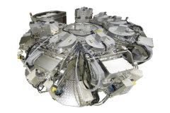 |
| Overhead view of the 8-chamber configuration (7 process chambers and a load-lock chamber) |
Abstract:
ULVAC, Inc. today announced the successful launch of PZT piezoelectric thin-film sputtering technology and a high volume manufacturing (HVM) solution to solve technical issues that have hindered the development of MEMS devices, which are crucial in applications from autonomous driving to next generation wearable terminals (such as smart glasses). The company has begun selling production systems incorporating the new technology.
ULVAC Launches Revolutionary PZT Piezoelectric Thin-film Process Technology and HVM Solution for MEMS Sensors/Actuators: Enabling Reliable, High-quality Film Production for Next Generation Devices
Chigasaki, Japan | Posted on August 16th, 2019Evolutions in technologies such as 5G and AI are expected to accelerate the journey towards smart societies, in which the digitization of all types of industries will improve industrial performance and enhance convenience for people. With increasing levels of multi-functionality found in autonomous driving, AR/VR, security, and smartphone applications, actuators are needed in order to activate devices based on signals received from various types of sensors. Demand for actuators is projected to explode and key issues in their development have come to the fore, including the need for miniaturization, reduced production costs, lower power consumption, and higher performance.
It used to be impossible to fabricate PZT piezoelectric thin films, which constitute the key technology in sensors and actuators, using a low-temperature process with the conventional coating method (Sol-Gel). However, in 2015, ULVAC successfully developed the world's most advanced technology for forming PZT piezoelectric thin films using a low-temperature sputtering process. ULVAC has continued developing this as next-generation MEMS technology.
By further advancing this proprietary technology, ULVAC has reduced running costs by optimizing system operation and has greatly improved the technology's reliability, which is critical for device commercialization. The result is a groundbreaking mass-production technology that is now incorporated into systems ULVAC has begun to sell.
This technology allows MEMS devices to be integrated with semiconductors (CMOS), and enables other positive outcomes such as miniaturization, reduced production costs, lower power consumption, and higher performance. It is expected to pave the way for increased use of MEMS devices in sensors and actuators in spatial information sensing and 3D image displays, including smart glasses. The technology will also facilitate MEMS device use in applications such as 3D fingerprint authentication.
ULVAC will continue to spearhead innovations in MEMS device technologies that can be used in a wide range of applications, including etching, sputtering, ashing, and sputtering targets. With all of these contributions, ULVAC plans to remain a driving force in the creation of smart societies.
Overview of the Technology
MEMS devices using thin-film PZT are formed on a silicon substrate with the following five (5) layers: an adhesion layer, a lower electrode layer, a buffer layer, a piezoelectric (PZT) layer, and an upper electrode layer. The laminated structure of all these layers can be formed using ULVAC's single-wafer sputtering system without exposing the substrate to the atmosphere. This multi-chamber sputtering system (model SME-200) allows for continuous process flow, optimizing each individual layer inside its own process chamber to achieve high repeatability and improved throughput. The system is also designed to provide a uniform and stable process for forming 8-inch silicon substrates, the largest size substrate available today for MEMS device mass production. A load-lock chamber and a maximum of seven (7) process chambers can be installed, including DC and RF magnetron sputtering chambers, and a rapid thermal annealing (RTA) chamber for accelerating crystallization.
ULVAC's PZT sputtering system uses PZT sputtering chambers specifically designed to solve problems unique to PZT, and it forms PZT thin films by growing crystals on a heated wafer. To do so, ULVAC uses a new low-temperature PZT thin-film process carried out at no more than 500 degrees C, as well as a proprietary process technology for applying a buffer layer, simultaneously achieving superior piezoelectric performance*1 and high reliability*2. Furthermore, through maintenance cycle optimization, running costs have been reduced to 75% of what they were in 2015, resulting in the world's highest PZT thin film performance under mass-production conditions.
Features of the Technology
1. Allows film formation by laminating individual layers inside the same system using a single-wafer sputtering system.
2. Achieves mass production of high-performance PZT thin films using a proprietary low-temperature process technology carried out at no more than 500 degrees C.
3. Achieves high device reliability through the use of a new process.
4. Reduces running costs to 75% of what they were in 2015.
*1 Piezoelectric performance: The higher the piezoelectric constant (e31), the greater the movement per unit of voltage applied to the device, making it possible to miniaturize the device and reduce its power consumption. (Piezoelectric constant e31: -15.5 C/m2 @ PZT film thickness: 2.0 um)
*2 High reliability: As indicators for the device's high level of durability, a dielectric breakdown voltage of around 200 V and a time-dependent dielectric breakdown (TDDB) of 2 million hours were confirmed.
####
About ULVAC, Inc.
ULVAC, Inc., founded in 1952, contributes to the development of industry through its comprehensive vacuum technologies. We created ULVAC SOLUTIONS based on these unique technologies and long years of research, development and production innovation. We offer these solutions, for equipment, materials, vacuum components, analytic evaluation and various other services, to manufacturers of electronic components, semiconductors, solar cells, flat panel displays and other industrial equipment.
For more information, please click here
Contacts:
ULVAC, Inc.
Advanced Electronics Equipment Division
TEL: +81-467-89-2139
Sales in Japan
ULVAC EQUIPMENT SALES, Inc.
Head Office (Tokyo) TEL: +81-3-5769-5511
Osaka Branch TEL: +81-6-6397-2281
Copyright © ULVAC, Inc.
If you have a comment, please Contact us.Issuers of news releases, not 7th Wave, Inc. or Nanotechnology Now, are solely responsible for the accuracy of the content.
Bookmark:


| Related News Press |
News and information
![]() Simulating magnetization in a Heisenberg quantum spin chain April 5th, 2024
Simulating magnetization in a Heisenberg quantum spin chain April 5th, 2024
![]() NRL charters Navy�s quantum inertial navigation path to reduce drift April 5th, 2024
NRL charters Navy�s quantum inertial navigation path to reduce drift April 5th, 2024
![]() Discovery points path to flash-like memory for storing qubits: Rice find could hasten development of nonvolatile quantum memory April 5th, 2024
Discovery points path to flash-like memory for storing qubits: Rice find could hasten development of nonvolatile quantum memory April 5th, 2024
![]() Good as gold - improving infectious disease testing with gold nanoparticles April 5th, 2024
Good as gold - improving infectious disease testing with gold nanoparticles April 5th, 2024
Thin films
![]() Utilizing palladium for addressing contact issues of buried oxide thin film transistors April 5th, 2024
Utilizing palladium for addressing contact issues of buried oxide thin film transistors April 5th, 2024
![]() Understanding the mechanism of non-uniform formation of diamond film on tools: Paving the way to a dry process with less environmental impact March 24th, 2023
Understanding the mechanism of non-uniform formation of diamond film on tools: Paving the way to a dry process with less environmental impact March 24th, 2023
![]() New study introduces the best graphite films: The work by Distinguished Professor Feng Ding at UNIST has been published in the October 2022 issue of Nature Nanotechnology November 4th, 2022
New study introduces the best graphite films: The work by Distinguished Professor Feng Ding at UNIST has been published in the October 2022 issue of Nature Nanotechnology November 4th, 2022
Wearable electronics
![]() CityU awarded invention: Soft, ultrathin photonic material cools down wearable electronic devices June 30th, 2023
CityU awarded invention: Soft, ultrathin photonic material cools down wearable electronic devices June 30th, 2023
![]() Liquid metal sticks to surfaces without a binding agent June 9th, 2023
Liquid metal sticks to surfaces without a binding agent June 9th, 2023
![]() Breaking through the limits of stretchable semiconductors with molecular brakes that harness light June 9th, 2023
Breaking through the limits of stretchable semiconductors with molecular brakes that harness light June 9th, 2023
![]() Tin selenide nanosheets enables to develop wearable tracking devices December 9th, 2022
Tin selenide nanosheets enables to develop wearable tracking devices December 9th, 2022
Internet-of-Things
![]() New nanowire sensors are the next step in the Internet of Things January 6th, 2023
New nanowire sensors are the next step in the Internet of Things January 6th, 2023
![]() New chip ramps up AI computing efficiency August 19th, 2022
New chip ramps up AI computing efficiency August 19th, 2022
Possible Futures
![]() Discovery points path to flash-like memory for storing qubits: Rice find could hasten development of nonvolatile quantum memory April 5th, 2024
Discovery points path to flash-like memory for storing qubits: Rice find could hasten development of nonvolatile quantum memory April 5th, 2024
![]() With VECSELs towards the quantum internet Fraunhofer: IAF achieves record output power with VECSEL for quantum frequency converters April 5th, 2024
With VECSELs towards the quantum internet Fraunhofer: IAF achieves record output power with VECSEL for quantum frequency converters April 5th, 2024
MEMS
![]() New Video Highlights Specific Topics Sought in Call for Papers for the 2019 IEEE International Electron Devices Meeting (IEDM) June 13th, 2019
New Video Highlights Specific Topics Sought in Call for Papers for the 2019 IEEE International Electron Devices Meeting (IEDM) June 13th, 2019
Chip Technology
![]() Discovery points path to flash-like memory for storing qubits: Rice find could hasten development of nonvolatile quantum memory April 5th, 2024
Discovery points path to flash-like memory for storing qubits: Rice find could hasten development of nonvolatile quantum memory April 5th, 2024
![]() Utilizing palladium for addressing contact issues of buried oxide thin film transistors April 5th, 2024
Utilizing palladium for addressing contact issues of buried oxide thin film transistors April 5th, 2024
![]() HKUST researchers develop new integration technique for efficient coupling of III-V and silicon February 16th, 2024
HKUST researchers develop new integration technique for efficient coupling of III-V and silicon February 16th, 2024
Announcements
![]() NRL charters Navy�s quantum inertial navigation path to reduce drift April 5th, 2024
NRL charters Navy�s quantum inertial navigation path to reduce drift April 5th, 2024
![]() Discovery points path to flash-like memory for storing qubits: Rice find could hasten development of nonvolatile quantum memory April 5th, 2024
Discovery points path to flash-like memory for storing qubits: Rice find could hasten development of nonvolatile quantum memory April 5th, 2024
Automotive/Transportation
![]() Researchers� approach may protect quantum computers from attacks March 8th, 2024
Researchers� approach may protect quantum computers from attacks March 8th, 2024
![]() Tests find no free-standing nanotubes released from tire tread wear September 8th, 2023
Tests find no free-standing nanotubes released from tire tread wear September 8th, 2023
Battery Technology/Capacitors/Generators/Piezoelectrics/Thermoelectrics/Energy storage
![]() What heat can tell us about battery chemistry: using the Peltier effect to study lithium-ion cells March 8th, 2024
What heat can tell us about battery chemistry: using the Peltier effect to study lithium-ion cells March 8th, 2024
![]() A battery�s hopping ions remember where they�ve been: Seen in atomic detail, the seemingly smooth flow of ions through a battery�s electrolyte is surprisingly complicated February 16th, 2024
A battery�s hopping ions remember where they�ve been: Seen in atomic detail, the seemingly smooth flow of ions through a battery�s electrolyte is surprisingly complicated February 16th, 2024
Artificial Intelligence
![]() Simulating magnetization in a Heisenberg quantum spin chain April 5th, 2024
Simulating magnetization in a Heisenberg quantum spin chain April 5th, 2024
![]() Researchers� approach may protect quantum computers from attacks March 8th, 2024
Researchers� approach may protect quantum computers from attacks March 8th, 2024
![]() New chip opens door to AI computing at light speed February 16th, 2024
New chip opens door to AI computing at light speed February 16th, 2024
![]() HKUST researchers develop new integration technique for efficient coupling of III-V and silicon February 16th, 2024
HKUST researchers develop new integration technique for efficient coupling of III-V and silicon February 16th, 2024
|
|
||
|
|
||
| The latest news from around the world, FREE | ||
|
|
||
|
|
||
| Premium Products | ||
|
|
||
|
Only the news you want to read!
Learn More |
||
|
|
||
|
Full-service, expert consulting
Learn More |
||
|
|
||