Home > Press > Functional Printing Enables Next Wave of Mass Produced Electronic
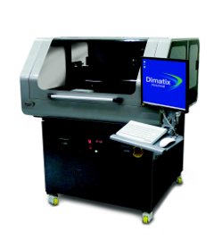 |
| Advanced ink-jet printing machine for the production of organic electronics. (Source: FUJIFILM Dimatix) |
Abstract:
LOPE-C - Functional Printing - May 31 to June 2, 2010 - Frankfurt, Germany
Functional Printing Enables Next Wave of Mass Produced Electronic
Frankfurt, Germany | Posted on January 20th, 2010Large-area, organic and printed electronics - complementing traditional silicon-based microelectronics - is at the threshold of mass production, promising a host of thin and lightweight, flexible and robust products. They are manufactured at very low cost by extending well established graphic printing techniques - layering very thin stacks of electronic components, semiconductors, insulators and barriers on polyester substrates. Functional printing enables a multitude of novel applications such as organic solar cells, OLED displays and wall-sized OLED lighting, e-readers, flat batteries, RFID tags, sensors and actuators for ambient intelligence in textiles and smart packaging, even low-cost electronic gadgets suited for one-time use - easily integrated in our familiar living surroundings.
LOPE-C 2010 (Large-area, Organic and Printed Electronics Convention), the annual conference and exhibition of the OE-A, held May 31 to June 2, 2010, at the Congress Center, Messe Frankfurt, Germany, will demonstrate the latest process technologies and applications to a worldwide audience of technologists, investors and end-users.
Low Cost Electronics: Printed Roll to Roll
Functional printing of mass-produced organic electronics is based on various rapidly evolving processes: flexographic printing, a subset of relief printing, transfers the ink from a printing form to plastic substrates. A variation of flexo is gravure printing, in which the printing pattern is defined by very small cups engraved in a printing cylinder. Gravure is a low-pressure technique enabling the use of organic dissolvent. Offset, a flat printing technique widely used for high-volume graphics and delivering excellent resolution at a very high throughput, is an additional option.
Screen printing is another high potential for mass producing organic electronics. Currently applied in PCB manufacturing, screen printing defines the printed pattern through an opaque mask applied to a fine mesh. By applying pressure the ink is forced onto the substrate in the non-masked areas. Rotary screen printing allows printing in thick layers, roll-to-roll. "Roll-to-roll printing opens up new opportunities for mass producing organic devices and systems," says Dr. Christian Maas of Werner Kammann Maschinenfabrik in B�nde, Germany. "High-end screen printing is a versatile basis for highly productive printing and coating applications." Among them, says Maas, are smooth and evenly spread electrodes for defibrillators, disposable glucose test strips, flexible batteries customizable for small portable products, antennas for RFID tags and automotive sealing devices.
A detailed overview of the various printing and patterning technologies as well as current and future applications is given in the "OE-A Roadmap for Organic and Printed Electronics" recently published by the Organic Electronics Association (OE-A).
Inkjet Printing for High Throughput Manufacturing
A strong contender for the printing of organic electronics is inkjet printing. Well known as a ubiquitous office appliance, inkjet uses very small droplets of ink, which are ejected onto the substrate through thermal or piezoelectric effects. Feature sizes of a few micrometers have been achieved. A very important, distinctive property of inkjet is that, due to its digital definition of the printed pattern, each subsequent impression can be different, allowing individual layouts and signatures.
"Inkjet has a bright future in the deposition of digital materials on organic substrates," says Martin Schoeppler, CEO and President of FUJIFILM Dimatix, Santa Clara, CA, USA. Using multiple printheads in parallel tremendously increases throughput - evolving inkjet to a high-quality mass printing technology. "The opportunities are unlimited," Mr. Schoeppler says, "ranging from polymer solar films, flexible polymer-based lighting elements, electronic books and paper-like electronic products to intelligent packaging featuring interactive displays and controls for consumer products."
Atmospheric and Vacuum Coating Processes
There is a host of other patterning techniques, such as laser ablation, vacuum deposition, soft lithography and large-area optical lithography, or solution coating techniques like slot-die, wire bar or curtain coating. Vacuum deposition processes show great potential for large-area roll-to-roll patterning and are pursued by Fraunhofer IPMS in Dresden, Germany. At its core is depositing functional layers for organic photovoltaics and OLED lighting devices on flexible substrates.
As an alternative, an atmospheric plasma-based powder coating technology for micro- and nanoparticle deposition has been developed by Reinhausen Plasma of Regensburg, Germany. "Plasmadust," as the process is called, works with materials such as Al, Cu, Zn and polymers, achieving high deposition rates at a low temperature load of the substrate. Among the applications are plasma and laser sintering, solar cell wafer metallization, and the manufacturing of thinfilm batteries and fuel cells.
Enabling Electronics Everywhere
Large-area, organic and printed electronics in its various production technologies is enabling vast opportunities for attractive consumer goods and intelligent packaging. Interactive periodicals, combining print and online content, are close to being introduced. Also on the agenda are medical applications, organic photovoltaics and lighting. The mid-term outlook for organic and printed electronics is evidenced in the current third edition of the official OE-A Roadmap White Paper. The latest progress in products and processes will be demonstrated hands-on at LOPE-C 2010.
####
About LOPE-C
LOPE-C (Large Area, Organic & Printed Electronics Convention) is the leading, fully industry-sponsored annual conferences and exhibition of organic and printed electronics. LOPE-C presents the economic trends and the scope of scientific achievements in the field. The convention focuses on the production and application of organic and printed electronics. LOPE-C 2010 is held May 31 to June 2, 2010 at the Congress Center of Messe Frankfurt, Germany. It is jointly organized by the Organic Electronics Association (OE-A) and Messe Frankfurt Ausstellungen GmbH.
About OE-A
Formed in 2004 as a Working Group within VDMA (German Engineering Federation), the OE-A (Organic Electronics Association) is the foremost professional body representing the worldwide organic and printed electronics industry. With more than 120 members throughout Europe, North America, Asia and Australia, OE-A represents the entire industrial value chain. The OE-A Roadmap, fixing time lines for applications and technologies, is now out in its third edition (2009). www.oe-a.org
About Messe Frankfurt Ausstellungen GmbH
Messe Frankfurt Ausstellungen GmbH is a fully owned subsidiary of Messe Frankfurt GmbH. At an annual turnover of �440m (2008), Messe Frankfurt is the world's largest fair company operating their own fair grounds. The globally active holding operates a worldwide network of 28 daughter companies, five branch offices and 52 international distribution partners and representatives. With this broad-based structure, Messe Frankfurt is present in more than 150 countries, with important industry events in more than 30 locations. In 2008, Messe Frankfurt organized a total of 102 fairs, 60 of which took place in foreign countries.
For more information, please click here
Contacts:
LOPE-C Press Contact:
For enquiries regarding LOPE-C 2010 conference topics and events, speaker interviews, etc. please
contact:
Werner Schulz
+49 (0) 30 81 05 89 59
Copyright © LOPE-C
If you have a comment, please Contact us.Issuers of news releases, not 7th Wave, Inc. or Nanotechnology Now, are solely responsible for the accuracy of the content.
Bookmark:


| Related News Press |
News and information
![]() Simulating magnetization in a Heisenberg quantum spin chain April 5th, 2024
Simulating magnetization in a Heisenberg quantum spin chain April 5th, 2024
![]() NRL charters Navy�s quantum inertial navigation path to reduce drift April 5th, 2024
NRL charters Navy�s quantum inertial navigation path to reduce drift April 5th, 2024
![]() Discovery points path to flash-like memory for storing qubits: Rice find could hasten development of nonvolatile quantum memory April 5th, 2024
Discovery points path to flash-like memory for storing qubits: Rice find could hasten development of nonvolatile quantum memory April 5th, 2024
![]() Good as gold - improving infectious disease testing with gold nanoparticles April 5th, 2024
Good as gold - improving infectious disease testing with gold nanoparticles April 5th, 2024
Display technology/LEDs/SS Lighting/OLEDs
![]() Utilizing palladium for addressing contact issues of buried oxide thin film transistors April 5th, 2024
Utilizing palladium for addressing contact issues of buried oxide thin film transistors April 5th, 2024
![]() Light guide plate based on perovskite nanocomposites November 3rd, 2023
Light guide plate based on perovskite nanocomposites November 3rd, 2023
![]() Simple ballpoint pen can write custom LEDs August 11th, 2023
Simple ballpoint pen can write custom LEDs August 11th, 2023
Chip Technology
![]() Discovery points path to flash-like memory for storing qubits: Rice find could hasten development of nonvolatile quantum memory April 5th, 2024
Discovery points path to flash-like memory for storing qubits: Rice find could hasten development of nonvolatile quantum memory April 5th, 2024
![]() Utilizing palladium for addressing contact issues of buried oxide thin film transistors April 5th, 2024
Utilizing palladium for addressing contact issues of buried oxide thin film transistors April 5th, 2024
![]() HKUST researchers develop new integration technique for efficient coupling of III-V and silicon February 16th, 2024
HKUST researchers develop new integration technique for efficient coupling of III-V and silicon February 16th, 2024
Sensors
Nanoelectronics
![]() Interdisciplinary: Rice team tackles the future of semiconductors Multiferroics could be the key to ultralow-energy computing October 6th, 2023
Interdisciplinary: Rice team tackles the future of semiconductors Multiferroics could be the key to ultralow-energy computing October 6th, 2023
![]() Key element for a scalable quantum computer: Physicists from Forschungszentrum J�lich and RWTH Aachen University demonstrate electron transport on a quantum chip September 23rd, 2022
Key element for a scalable quantum computer: Physicists from Forschungszentrum J�lich and RWTH Aachen University demonstrate electron transport on a quantum chip September 23rd, 2022
![]() Reduced power consumption in semiconductor devices September 23rd, 2022
Reduced power consumption in semiconductor devices September 23rd, 2022
![]() Atomic level deposition to extend Moore�s law and beyond July 15th, 2022
Atomic level deposition to extend Moore�s law and beyond July 15th, 2022
Announcements
![]() NRL charters Navy�s quantum inertial navigation path to reduce drift April 5th, 2024
NRL charters Navy�s quantum inertial navigation path to reduce drift April 5th, 2024
![]() Discovery points path to flash-like memory for storing qubits: Rice find could hasten development of nonvolatile quantum memory April 5th, 2024
Discovery points path to flash-like memory for storing qubits: Rice find could hasten development of nonvolatile quantum memory April 5th, 2024
Automotive/Transportation
![]() Researchers� approach may protect quantum computers from attacks March 8th, 2024
Researchers� approach may protect quantum computers from attacks March 8th, 2024
![]() Tests find no free-standing nanotubes released from tire tread wear September 8th, 2023
Tests find no free-standing nanotubes released from tire tread wear September 8th, 2023
Textiles/Clothing
![]() Protective equipment with graphene nanotubes meets the strictest ESD safety standards March 25th, 2022
Protective equipment with graphene nanotubes meets the strictest ESD safety standards March 25th, 2022
![]() Polymer fibers with graphene nanotubes make it possible to heat hard-to-reach, complex-shaped items February 11th, 2022
Polymer fibers with graphene nanotubes make it possible to heat hard-to-reach, complex-shaped items February 11th, 2022
![]() Flexible material shows potential for use in fabrics to heat, cool July 3rd, 2020
Flexible material shows potential for use in fabrics to heat, cool July 3rd, 2020
Battery Technology/Capacitors/Generators/Piezoelectrics/Thermoelectrics/Energy storage
![]() What heat can tell us about battery chemistry: using the Peltier effect to study lithium-ion cells March 8th, 2024
What heat can tell us about battery chemistry: using the Peltier effect to study lithium-ion cells March 8th, 2024
![]() A battery�s hopping ions remember where they�ve been: Seen in atomic detail, the seemingly smooth flow of ions through a battery�s electrolyte is surprisingly complicated February 16th, 2024
A battery�s hopping ions remember where they�ve been: Seen in atomic detail, the seemingly smooth flow of ions through a battery�s electrolyte is surprisingly complicated February 16th, 2024
Events/Classes
![]() Researchers demonstrate co-propagation of quantum and classical signals: Study shows that quantum encryption can be implemented in existing fiber networks January 20th, 2023
Researchers demonstrate co-propagation of quantum and classical signals: Study shows that quantum encryption can be implemented in existing fiber networks January 20th, 2023
Solar/Photovoltaic
![]() Development of zinc oxide nanopagoda array photoelectrode: photoelectrochemical water-splitting hydrogen production January 12th, 2024
Development of zinc oxide nanopagoda array photoelectrode: photoelectrochemical water-splitting hydrogen production January 12th, 2024
![]() Shedding light on unique conduction mechanisms in a new type of perovskite oxide November 17th, 2023
Shedding light on unique conduction mechanisms in a new type of perovskite oxide November 17th, 2023
![]() Inverted perovskite solar cell breaks 25% efficiency record: Researchers improve cell efficiency using a combination of molecules to address different November 17th, 2023
Inverted perovskite solar cell breaks 25% efficiency record: Researchers improve cell efficiency using a combination of molecules to address different November 17th, 2023
![]() Charged �molecular beasts� the basis for new compounds: Researchers at Leipzig University use �aggressive� fragments of molecular ions for chemical synthesis November 3rd, 2023
Charged �molecular beasts� the basis for new compounds: Researchers at Leipzig University use �aggressive� fragments of molecular ions for chemical synthesis November 3rd, 2023
|
|
||
|
|
||
| The latest news from around the world, FREE | ||
|
|
||
|
|
||
| Premium Products | ||
|
|
||
|
Only the news you want to read!
Learn More |
||
|
|
||
|
Full-service, expert consulting
Learn More |
||
|
|
||