Home > Press > Thermochemical nanopatterning of organic semiconductors
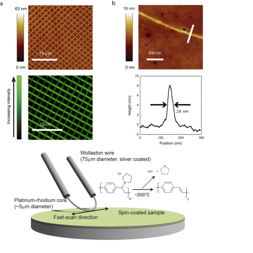 |
| Figure � A schematic of the Wollaston wire probe and the lithographic process (bottom). a Regular patterns drawn over large areas using scanning thermochemical lithography. The top image is an atomic force micrograph, whilst the bottom image is from a confocal microscope. b Atomic force microscope image of a high resolution lithographic line (top) and its cross-section (bottom). |
Abstract:
Researchers from the London Centre for Nanotechnology (LCN) and University College London (UCL) have fabricated sub-30 nm luminescent features of an organic semiconductor via spatially selective conversion and patterning of its precursor by using a heatable, micron-size scanning probe (see figure below). The results will soon be reported in the journal Nature Nanotechnology.
Thermochemical nanopatterning of organic semiconductors
London | Posted on September 8th, 2009The future development of electronics and photonics relies on a range of sophisticated lithographyic techniques for the patterning of semiconducting, dielectric, and metallic materials. Researchers at the London Centre of Nanotechnology (LCN), the Department of Physics and Astronomy, and the Eastman Dental Institute at UCL, have now developed a thermochemical patterning technique for materials known as organic semiconductors.
These materials can be used in light-emitting diodes (LEDs), solar cells, lasers and transistors, and their potential is in low processing costs and the ability to build devices on flexible substrates. However, applications of these materials in nanoelectronics and nanophotonics are limited by the range of patterning techniques available. Many of the approaches to nanolithography that are used to pattern inorganic materials, such as e-beams or Focused Ion Beams (FIBs), are too harsh for organic semiconductors, that can be damaged by the high energy of the patterning beams, or by the chemicals needed for the processing.
So, instead of using standard optical or other "conventional" high-resolution lithographies, the UCL researchers used a small heat source for the patterning. This heat source, known as a modified Wollaston wire, can be mounted on an atomic force microscope and scanned across surfaces to chemically convert all areas it comes into contact with. This technique has allowed the UCL researchers to achieve patterned resolutions below 28 nm and write speeds of 100 �m/s in the widely used organic semiconductor, PPV. The result is particularly surprising given the large diameter of the heat source (5 �m) compared to the resolutions achieved, and since it is likely that resolution could be further improved with the use of nanoscale heat sources, as already reported by other groups.
There has already been some commercial interest in using atomic force microscopes to pattern surfaces, as for example by IBM in their �millipede' project, that was aimed at data-storage applications, but such a thermochemical approach opens up new possibilities. In particular, this work shows that thermochemical lithography offers a versatile, simple and reliable nanopatterning technique. For example, thermo-crosslinkable additives could easily be added to a variety of other solution-processible semiconductors. The technique should also be generally applicable to other classes of materials. A large number of optical materials, including many commercial cross-linker additives and photoresists, rely in fact on chemical mechanisms that can also be thermally activated.
The group, led by Franco Cacialli, has previously used scanning near-field optical lithography (SNOL) for nanopatterning of PPV structures from the same precursor polymer, poly(p-xylene tetrahydrothiophenium chloride) (PXT). This work included the fabrication of quasi-periodic two-dimensional structures with potential for photonic applications. However, the thermochemical technique now developed (Scanning Thermal lithography, or SThL) enables one to bypass the UV insolubilisation step, and the complications and additional costs imposed by the needs for lasers, optics, and sophisticated optical fibre probes.
More details regarding the research in the Organic Semiconductors Group led by Franco Cacialli can be found at the website: www.cmmp.ucl.ac.uk/~fc/OS/
####
About London Centre for Nanotechnology (LCN)
The London Centre for Nanotechnology, LCN, is a UK based multidisciplinary enterprise operating at the forefront of science and technology. It is a joint venture between University College London and Imperial College London and is based at the Bloomsbury and South Kensington sites. It has a unique operating model that accesses and focusses the combined skills of the departments of chemistry, physics, materials, medicine, electrical and electronic engineering, mechanical engineering, chemical engineering, biochemical engineering and earth sciences across the two universities.
For more information, please click here
Contacts:
Bloomsbury (UCL) Site
London Centre for Nanotechnology
17-19 Gordon Street
London WC1H 0AH
tel: +44 (0)20 7679 0604
fax: +44 (0)20 7679 0595
Copyright © London Centre for Nanotechnology (LCN)
If you have a comment, please Contact us.Issuers of news releases, not 7th Wave, Inc. or Nanotechnology Now, are solely responsible for the accuracy of the content.
Bookmark:


| Related News Press |
News and information
![]() Simulating magnetization in a Heisenberg quantum spin chain April 5th, 2024
Simulating magnetization in a Heisenberg quantum spin chain April 5th, 2024
![]() NRL charters Navy�s quantum inertial navigation path to reduce drift April 5th, 2024
NRL charters Navy�s quantum inertial navigation path to reduce drift April 5th, 2024
![]() Discovery points path to flash-like memory for storing qubits: Rice find could hasten development of nonvolatile quantum memory April 5th, 2024
Discovery points path to flash-like memory for storing qubits: Rice find could hasten development of nonvolatile quantum memory April 5th, 2024
![]() Good as gold - improving infectious disease testing with gold nanoparticles April 5th, 2024
Good as gold - improving infectious disease testing with gold nanoparticles April 5th, 2024
Display technology/LEDs/SS Lighting/OLEDs
![]() Utilizing palladium for addressing contact issues of buried oxide thin film transistors April 5th, 2024
Utilizing palladium for addressing contact issues of buried oxide thin film transistors April 5th, 2024
![]() Light guide plate based on perovskite nanocomposites November 3rd, 2023
Light guide plate based on perovskite nanocomposites November 3rd, 2023
![]() Simple ballpoint pen can write custom LEDs August 11th, 2023
Simple ballpoint pen can write custom LEDs August 11th, 2023
Chip Technology
![]() Discovery points path to flash-like memory for storing qubits: Rice find could hasten development of nonvolatile quantum memory April 5th, 2024
Discovery points path to flash-like memory for storing qubits: Rice find could hasten development of nonvolatile quantum memory April 5th, 2024
![]() Utilizing palladium for addressing contact issues of buried oxide thin film transistors April 5th, 2024
Utilizing palladium for addressing contact issues of buried oxide thin film transistors April 5th, 2024
![]() HKUST researchers develop new integration technique for efficient coupling of III-V and silicon February 16th, 2024
HKUST researchers develop new integration technique for efficient coupling of III-V and silicon February 16th, 2024
Nanoelectronics
![]() Interdisciplinary: Rice team tackles the future of semiconductors Multiferroics could be the key to ultralow-energy computing October 6th, 2023
Interdisciplinary: Rice team tackles the future of semiconductors Multiferroics could be the key to ultralow-energy computing October 6th, 2023
![]() Key element for a scalable quantum computer: Physicists from Forschungszentrum J�lich and RWTH Aachen University demonstrate electron transport on a quantum chip September 23rd, 2022
Key element for a scalable quantum computer: Physicists from Forschungszentrum J�lich and RWTH Aachen University demonstrate electron transport on a quantum chip September 23rd, 2022
![]() Reduced power consumption in semiconductor devices September 23rd, 2022
Reduced power consumption in semiconductor devices September 23rd, 2022
![]() Atomic level deposition to extend Moore�s law and beyond July 15th, 2022
Atomic level deposition to extend Moore�s law and beyond July 15th, 2022
Announcements
![]() NRL charters Navy�s quantum inertial navigation path to reduce drift April 5th, 2024
NRL charters Navy�s quantum inertial navigation path to reduce drift April 5th, 2024
![]() Discovery points path to flash-like memory for storing qubits: Rice find could hasten development of nonvolatile quantum memory April 5th, 2024
Discovery points path to flash-like memory for storing qubits: Rice find could hasten development of nonvolatile quantum memory April 5th, 2024
Tools
![]() Ferroelectrically modulate the Fermi level of graphene oxide to enhance SERS response November 3rd, 2023
Ferroelectrically modulate the Fermi level of graphene oxide to enhance SERS response November 3rd, 2023
![]() The USTC realizes In situ electron paramagnetic resonance spectroscopy using single nanodiamond sensors November 3rd, 2023
The USTC realizes In situ electron paramagnetic resonance spectroscopy using single nanodiamond sensors November 3rd, 2023
Photonics/Optics/Lasers
![]() With VECSELs towards the quantum internet Fraunhofer: IAF achieves record output power with VECSEL for quantum frequency converters April 5th, 2024
With VECSELs towards the quantum internet Fraunhofer: IAF achieves record output power with VECSEL for quantum frequency converters April 5th, 2024
![]() Nanoscale CL thermometry with lanthanide-doped heavy-metal oxide in TEM March 8th, 2024
Nanoscale CL thermometry with lanthanide-doped heavy-metal oxide in TEM March 8th, 2024
![]() Optically trapped quantum droplets of light can bind together to form macroscopic complexes March 8th, 2024
Optically trapped quantum droplets of light can bind together to form macroscopic complexes March 8th, 2024
![]() HKUST researchers develop new integration technique for efficient coupling of III-V and silicon February 16th, 2024
HKUST researchers develop new integration technique for efficient coupling of III-V and silicon February 16th, 2024
Solar/Photovoltaic
![]() Development of zinc oxide nanopagoda array photoelectrode: photoelectrochemical water-splitting hydrogen production January 12th, 2024
Development of zinc oxide nanopagoda array photoelectrode: photoelectrochemical water-splitting hydrogen production January 12th, 2024
![]() Shedding light on unique conduction mechanisms in a new type of perovskite oxide November 17th, 2023
Shedding light on unique conduction mechanisms in a new type of perovskite oxide November 17th, 2023
![]() Inverted perovskite solar cell breaks 25% efficiency record: Researchers improve cell efficiency using a combination of molecules to address different November 17th, 2023
Inverted perovskite solar cell breaks 25% efficiency record: Researchers improve cell efficiency using a combination of molecules to address different November 17th, 2023
![]() Charged �molecular beasts� the basis for new compounds: Researchers at Leipzig University use �aggressive� fragments of molecular ions for chemical synthesis November 3rd, 2023
Charged �molecular beasts� the basis for new compounds: Researchers at Leipzig University use �aggressive� fragments of molecular ions for chemical synthesis November 3rd, 2023
|
|
||
|
|
||
| The latest news from around the world, FREE | ||
|
|
||
|
|
||
| Premium Products | ||
|
|
||
|
Only the news you want to read!
Learn More |
||
|
|
||
|
Full-service, expert consulting
Learn More |
||
|
|
||