Home > Press > Unraveling the origin of extremely bright quantum emitters: Researchers from Osaka University have discovered the fundamental properties of single-photon emitters at an oxide/semiconductor interface, which could be crucial for scalable quantum technology
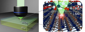 |
| Schematic of light emission from the color center at the oxide/SiC interface Credit Osaka University |
Abstract:
Many next-generation quantum devices rely on single-photon emitters based on optically active defects in solids, known as color centers. Understanding their properties is fundamental to developing novel quantum technologies.
Unraveling the origin of extremely bright quantum emitters: Researchers from Osaka University have discovered the fundamental properties of single-photon emitters at an oxide/semiconductor interface, which could be crucial for scalable quantum technology
Osaka, Japan | Posted on February 28th, 2025Now, in a study published in APL Materials, a multi-institutional research team led by Osaka University has sought to clarify the origin of the extremely bright color centers at the interface between silicon dioxide (SiO2) and silicon carbide (SiC).
Previous research has demonstrated a range of factors that can play a role in the formation of these interface color centers, including the effect of annealing after oxidation. However, the energy level structure (i.e., the electronic transitions taking place) responsible for luminescence, a crucial factor for understanding the origin of color centers, was completely unknown.
�The origin of color centers at the SiO2/SiC interface has posed a long-standing research problem, and its discovery could boost the development of scalable quantum technologies,� explains Kentaro Onishi, lead author of the study.
In this study, the researchers were able to determine the energy levels of color centers at the SiO2/SiC interface. These particular color centers are formed by oxidizing the SiC substrate. Energy levels are formed in the forbidden energy gap of a semiconductor by defects that trap electrons, known as electron traps.
The oxidation conditions during fabrication, including temperature and partial pressure, were thought to influence the densities of color centers and electron traps at the interface, but this work presents the first detailed investigation of the effect of these conditions over a wide range.
The researchers observed a clear correlation between the luminescence of color centers and the density of electron traps, discovering their common origin. The color centers were associated with a specific energy level (i.e., 0.65�0.92 eV from the conduction band edge of SiC), and after comparing the experimental results with theoretical studies, the researchers suggest a specific carbon-related defect as the most promising candidate of the color centers.
�Our results are exciting because we are finally beginning to understand how these interface color centers come to be and how their luminescence works,� says Takuma Kobayashi, senior author of the study. �As we deepen our understanding, our hope grows for the realization of quantum technologies using interface color centers. Since these color centers are at the heart of metal-oxide-semiconductor devices, the high compatibility with evolving large-scale integration technologies should pave the way for scalable quantum applications.�
As quantum technology relies on the precise control of color centers, this research represents a step toward being able to fabricate such quantum devices in the future.
####
About Osaka University
Osaka University was founded in 1931 as one of the seven imperial universities of Japan and is now one of Japan's leading comprehensive universities with a broad disciplinary spectrum. This strength is coupled with a singular drive for innovation that extends throughout the scientific process, from fundamental research to the creation of applied technology with positive economic impacts. Its commitment to innovation has been recognized in Japan and around the world. Now, Osaka University is leveraging its role as a Designated National University Corporation selected by the Ministry of Education, Culture, Sports, Science and Technology to contribute to innovation for human welfare, sustainable development of society, and social transformation.
For more information, please click here
Contacts:
Saori Obayashi
Osaka University
Office: 81-661-055-886
Copyright © Osaka University
If you have a comment, please Contact us.Issuers of news releases, not 7th Wave, Inc. or Nanotechnology Now, are solely responsible for the accuracy of the content.
Bookmark:


| Related Links |
| Related News Press |
News and information
![]() Quantum computer improves AI predictions April 17th, 2026
Quantum computer improves AI predictions April 17th, 2026
![]() Flexible sensor gains sensitivity under pressure April 17th, 2026
Flexible sensor gains sensitivity under pressure April 17th, 2026
![]() A reusable chip for particulate matter sensing April 17th, 2026
A reusable chip for particulate matter sensing April 17th, 2026
![]() Detecting vibrational quantum beating in the predissociation dynamics of SF6 using time-resolved photoelectron spectroscopy April 17th, 2026
Detecting vibrational quantum beating in the predissociation dynamics of SF6 using time-resolved photoelectron spectroscopy April 17th, 2026
Quantum Physics
![]() Detecting vibrational quantum beating in the predissociation dynamics of SF6 using time-resolved photoelectron spectroscopy April 17th, 2026
Detecting vibrational quantum beating in the predissociation dynamics of SF6 using time-resolved photoelectron spectroscopy April 17th, 2026
![]() Beyond silicon: Electronics at the scale of a single molecule January 30th, 2026
Beyond silicon: Electronics at the scale of a single molecule January 30th, 2026
Possible Futures
![]() A fundamentally new therapeutic approach to cystic fibrosis: Nanobody repairs cellular defect April 17th, 2026
A fundamentally new therapeutic approach to cystic fibrosis: Nanobody repairs cellular defect April 17th, 2026
![]() UC Irvine physicists discover method to reverse �quantum scrambling� : The work addresses the problem of information loss in quantum computing system April 17th, 2026
UC Irvine physicists discover method to reverse �quantum scrambling� : The work addresses the problem of information loss in quantum computing system April 17th, 2026
Discoveries
![]() Quantum computer improves AI predictions April 17th, 2026
Quantum computer improves AI predictions April 17th, 2026
![]() Flexible sensor gains sensitivity under pressure April 17th, 2026
Flexible sensor gains sensitivity under pressure April 17th, 2026
![]() A reusable chip for particulate matter sensing April 17th, 2026
A reusable chip for particulate matter sensing April 17th, 2026
![]() Detecting vibrational quantum beating in the predissociation dynamics of SF6 using time-resolved photoelectron spectroscopy April 17th, 2026
Detecting vibrational quantum beating in the predissociation dynamics of SF6 using time-resolved photoelectron spectroscopy April 17th, 2026
Announcements
![]() A fundamentally new therapeutic approach to cystic fibrosis: Nanobody repairs cellular defect April 17th, 2026
A fundamentally new therapeutic approach to cystic fibrosis: Nanobody repairs cellular defect April 17th, 2026
![]() UC Irvine physicists discover method to reverse �quantum scrambling� : The work addresses the problem of information loss in quantum computing system April 17th, 2026
UC Irvine physicists discover method to reverse �quantum scrambling� : The work addresses the problem of information loss in quantum computing system April 17th, 2026
Interviews/Book Reviews/Essays/Reports/Podcasts/Journals/White papers/Posters
![]() A fundamentally new therapeutic approach to cystic fibrosis: Nanobody repairs cellular defect April 17th, 2026
A fundamentally new therapeutic approach to cystic fibrosis: Nanobody repairs cellular defect April 17th, 2026
![]() UC Irvine physicists discover method to reverse �quantum scrambling� : The work addresses the problem of information loss in quantum computing system April 17th, 2026
UC Irvine physicists discover method to reverse �quantum scrambling� : The work addresses the problem of information loss in quantum computing system April 17th, 2026
Quantum nanoscience
![]() Beyond silicon: Electronics at the scale of a single molecule January 30th, 2026
Beyond silicon: Electronics at the scale of a single molecule January 30th, 2026
![]() MXene nanomaterials enter a new dimension Multilayer nanomaterial: MXene flakes created at Drexel University show new promise as 1D scrolls January 30th, 2026
MXene nanomaterials enter a new dimension Multilayer nanomaterial: MXene flakes created at Drexel University show new promise as 1D scrolls January 30th, 2026
![]() ICFO researchers overcome long-standing bottleneck in single photon detection with twisted 2D materials August 8th, 2025
ICFO researchers overcome long-standing bottleneck in single photon detection with twisted 2D materials August 8th, 2025
|
|
||
|
|
||
| The latest news from around the world, FREE | ||
|
|
||
|
|
||
| Premium Products | ||
|
|
||
|
Only the news you want to read!
Learn More |
||
|
|
||
|
Full-service, expert consulting
Learn More |
||
|
|
||