Home > Press > Successful morphing of inorganic perovskites without damaging their functional properties
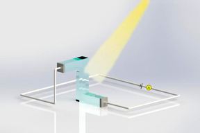 |
| Applying morphed perovskites to construct an innovative photodetector. CREDIT �Dr Li Xiaocui / City University of Hong Kong |
Abstract:
A research team co-led by scholars from City University of Hong Kong (CityU) has successfully morphed all-inorganic perovskites at room temperature without compromising their functional properties. Their findings demonstrate the potential of this class of semiconductors for manufacturing next-generation deformable electronics and energy systems in the future.
Successful morphing of inorganic perovskites without damaging their functional properties
Hong Kong, China | Posted on October 6th, 2023All-inorganic lead halide perovskites are becoming increasingly important semiconducting materials in energy conversion and optoelectronics because of their outstanding performance and enhanced environmental stability.
�However, unlike metal materials or polymers, inorganic semiconductors are often brittle and hard to process. This strongly restricts their applications as optoelectronic products that must withstand mechanical stress and strain without losing their functionality,� said Professor Chen Fu-Rong, Associate Vice-President (Mainland Collaboration) and Chair Professor of Materials Science at CityU, who co-led the study.
To overcome this limitation, a research team led by Professor Chen, along with Professor Johnny Ho Chung-yin, Associate Head and Professor in the Department of Materials Science and Engineering (MSE), Professor Zhao Shijun, in the Department of Mechanical Engineering (MNE) at CityU, and Professor Lu Yang, former professor in MNE and currently working at The University of Hong Kong (HKU), explored the deformability of all-inorganic perovskites (CsPbX3, where X can be Cl, Br or I ions). They found perovskites can be substantially morphed into distinct geometries at room temperature while preserving their functional properties, an achievement unprecedented in conventional inorganic semiconductors.
In their experiments, the team first synthesized single-crystal micropillars of CsPbX3 with diameters and widths ranging from 0.4 to 2 μm and lengths of 3 to 10 μm, using the vapour-liquid-solid method. They then conducted in situ compression experiments with a scanning electron microscope.
They found that under compression, there were continuous slips of partial dislocations on multiple slip systems in the CsPbX3 crystal lattice. This �domino-like� multi-slipping deformation mechanism enabled the micropillars to deform into various distinct shapes without fracturing, including upside-down L shape, Z shape, and wine-glass shape.
With the aid of an atomic-resolution transmission electron microscope (TEM), the team revealed that the atoms in the deformation zone were well connected, leading to undamaged functional properties. �We also observed that the optoelectronic performance of the micropillars remained unaffected by the deformation,� said Professor Ho. �This demonstrates the potential of these materials for use in deformable optoelectronics.�
The research team performed further electronic and structural analyses to uncover the physical origin of this unusual behaviour. �The secret of the morphing ability is the low-slip energy barrier, which ensures facile slips, and the strong Pb�X bonds, which maintain the crystal�s structural integrity and prevent cracking or cleaving,� said Professor Zhao Shijun, who specializes in the properties of computational materials. And the bandgap � an energy index influencing the total electrical properties of intrinsic semiconductors � of the CsPbX3 crystal lattice remained unchanged after deformation, indicating that the electronic structure of the material was unaffected, he added.
�Our results demonstrated that all-inorganic CsPbX3 single crystals can be substantially deformed and facilely morphed into various shapes through multi-slipping under ambient conditions, without changing their crystalline integrity, lattice structure or optoelectronic properties,� said Professor Chen.
�This achievement represents a significant step towards designing and manufacturing innovative energy devices and deformable electronics. The underlying mechanism, uncovered by a TEM at the atomic level provides important implications for seeking other intrinsic ductile semiconductors,� he added.
The findings were published in Nature Materials under the title �Multislip-enabled morphing of all-inorganic perovskites�.
The first authors are Dr Li Xiaocui, Dr Meng You and Dr Li Wanpeng, postdocs in the MSE Department. The corresponding authors are Professor Chen, Professor Ho, Professor Zhao, and Professor Lu of HKU. Other collaborators are researchers from CityU and Zhejiang University.
The research is supported by the Hong Kong Research Grants Council (RGC), CityU, and the National Natural Science Foundation of China/RGC Hong Kong Joint Research Scheme.
####
For more information, please click here
Contacts:
P.K. Lee
City University of Hong Kong
Office: 852-344-28925
Copyright © City University of Hong Kong
If you have a comment, please Contact us.Issuers of news releases, not 7th Wave, Inc. or Nanotechnology Now, are solely responsible for the accuracy of the content.
Bookmark:


| Related Links |
| Related News Press |
News and information
![]() Researchers develop molecular qubits that communicate at telecom frequencies October 3rd, 2025
Researchers develop molecular qubits that communicate at telecom frequencies October 3rd, 2025
![]() Next-generation quantum communication October 3rd, 2025
Next-generation quantum communication October 3rd, 2025
![]() "Nanoreactor" cage uses visible light for catalytic and ultra-selective cross-cycloadditions October 3rd, 2025
"Nanoreactor" cage uses visible light for catalytic and ultra-selective cross-cycloadditions October 3rd, 2025
Perovskites
Possible Futures
![]() Spinel-type sulfide semiconductors to operate the next-generation LEDs and solar cells For solar-cell absorbers and green-LED source October 3rd, 2025
Spinel-type sulfide semiconductors to operate the next-generation LEDs and solar cells For solar-cell absorbers and green-LED source October 3rd, 2025
Chip Technology
![]() Lab to industry: InSe wafer-scale breakthrough for future electronics August 8th, 2025
Lab to industry: InSe wafer-scale breakthrough for future electronics August 8th, 2025
![]() A 1960s idea inspires NBI researchers to study hitherto inaccessible quantum states June 6th, 2025
A 1960s idea inspires NBI researchers to study hitherto inaccessible quantum states June 6th, 2025
![]() Programmable electron-induced color router array May 14th, 2025
Programmable electron-induced color router array May 14th, 2025
Optical computing/Photonic computing
![]() ICFO researchers overcome long-standing bottleneck in single photon detection with twisted 2D materials August 8th, 2025
ICFO researchers overcome long-standing bottleneck in single photon detection with twisted 2D materials August 8th, 2025
![]() Programmable electron-induced color router array May 14th, 2025
Programmable electron-induced color router array May 14th, 2025
![]() Nanophotonic platform boosts efficiency of nonlinear-optical quantum teleportation April 25th, 2025
Nanophotonic platform boosts efficiency of nonlinear-optical quantum teleportation April 25th, 2025
![]() Groundbreaking research unveils unified theory for optical singularities in photonic microstructures December 13th, 2024
Groundbreaking research unveils unified theory for optical singularities in photonic microstructures December 13th, 2024
Discoveries
![]() Researchers develop molecular qubits that communicate at telecom frequencies October 3rd, 2025
Researchers develop molecular qubits that communicate at telecom frequencies October 3rd, 2025
![]() Next-generation quantum communication October 3rd, 2025
Next-generation quantum communication October 3rd, 2025
![]() "Nanoreactor" cage uses visible light for catalytic and ultra-selective cross-cycloadditions October 3rd, 2025
"Nanoreactor" cage uses visible light for catalytic and ultra-selective cross-cycloadditions October 3rd, 2025
Announcements
![]() Rice membrane extracts lithium from brines with greater speed, less waste October 3rd, 2025
Rice membrane extracts lithium from brines with greater speed, less waste October 3rd, 2025
![]() Researchers develop molecular qubits that communicate at telecom frequencies October 3rd, 2025
Researchers develop molecular qubits that communicate at telecom frequencies October 3rd, 2025
![]() Next-generation quantum communication October 3rd, 2025
Next-generation quantum communication October 3rd, 2025
![]() "Nanoreactor" cage uses visible light for catalytic and ultra-selective cross-cycloadditions October 3rd, 2025
"Nanoreactor" cage uses visible light for catalytic and ultra-selective cross-cycloadditions October 3rd, 2025
Interviews/Book Reviews/Essays/Reports/Podcasts/Journals/White papers/Posters
![]() Spinel-type sulfide semiconductors to operate the next-generation LEDs and solar cells For solar-cell absorbers and green-LED source October 3rd, 2025
Spinel-type sulfide semiconductors to operate the next-generation LEDs and solar cells For solar-cell absorbers and green-LED source October 3rd, 2025
![]() Rice membrane extracts lithium from brines with greater speed, less waste October 3rd, 2025
Rice membrane extracts lithium from brines with greater speed, less waste October 3rd, 2025
Energy
![]() Sensors innovations for smart lithium-based batteries: advancements, opportunities, and potential challenges August 8th, 2025
Sensors innovations for smart lithium-based batteries: advancements, opportunities, and potential challenges August 8th, 2025
![]() Simple algorithm paired with standard imaging tool could predict failure in lithium metal batteries August 8th, 2025
Simple algorithm paired with standard imaging tool could predict failure in lithium metal batteries August 8th, 2025
|
|
||
|
|
||
| The latest news from around the world, FREE | ||
|
|
||
|
|
||
| Premium Products | ||
|
|
||
|
Only the news you want to read!
Learn More |
||
|
|
||
|
Full-service, expert consulting
Learn More |
||
|
|
||