Home > Press > Wafer-scale 2D MoTe₂ layers enable highly-sensitive broadband integrated infrared detector
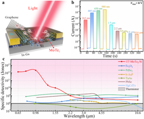 |
| a, Schematic illustration of a graphene/1Tʹ-MoTe₂/Si Schottky junction device. b,Time-dependent photoresponse properties to pulsed light illumination in a broad spectral band. c, Comparison of the room-temperature specific detectivity of the Gr/1Tʹ-MoTe₂/Si Schottky junction device with other devices. CREDIT by Di Wu, Chenguang Guo, Longhui Zeng, Xiaoyan Ren, Zhifeng Shi, Long Wen, Qin Chen, Meng Zhang, Xin Jian Li, Chong-Xin Shan, and Jiansheng Jie |
Abstract:
Detection in multiple infrared (IR) regions spanning from short- and mid- to long-wave IR plays an important role in diverse fields from scientific research to wide-ranging technological applications including target identification, imaging, remote monitoring, and gas sensing. Currently, the state-of-the-art IR photodetectors are mainly dominated by conventional narrow bandgap semiconductors including In1-xGaxAs, InSb, and Hg1-xCdxTe, operating in short-wave IR (SWIR, 1-3 µm), mid-wave IR (MWIR, 3-6 µm), and long-wave IR (LWIR, 6-15 µm) spectral bands, respectively. Notably, these photodetectors not only rely on high-temperature growth process of raw materials and complex processing technique, but also suffer from the cryogenic cooling conditions with time-consuming and high power consumption. Moreover, there are several remaining technological challenges such as poor complementary metal-oxide-semiconductor (CMOS) compatibility, bulky module size, and low efficiency, which severely restrict the wider application of these detectors.
Wafer-scale 2D MoTe₂ layers enable highly-sensitive broadband integrated infrared detector
Changchun, China | Posted on January 6th, 2023In a new paper published in Light Science & Application, Prof. Di Wu and Xinjian Li from Zhengzhou University, Dr. Longhui Zeng from the University of California-San Diego, and Prof. Jiansheng Jie from Soochow University demonstrated a facile thermal-assisted tellurization route for the van der Waals (vdW) growth of wafer-scale phase-controlled 2D MoTe2 layers. The type-II Weyl semimetal 1T′-MoTe2 layers were directly deposited on prepatterned Si substrate to in-situ fabricate 1T'-MoTe2/Si vertical Schottky junction. The high-quality Schottky junction interface and vertical device structure with graphene electrode ensure efficient carrier transport and reduce carrier recombination, enabling the detector to achieve an ultrabroadband detection range of up to 10.6 μm and a room-temperature specific detectivity of over 108 Jones in the mid-infrared region. The wafer-scale 2D MoTe2 layers have also enabled the integrated device array to be successfully implemented for high-resolution uncooled mid-infrared imaging.
In this study, a pre-deposited Mo film as a precursor was transformed to 2D MoTe2 layer via vdW growth mechanism through a direct thermal-assisted tellurization process. As a matter of fact, the phase transition of MoTe2 is highly dependent on the growth time. By controlling the growth time, 2-inch 2H and 1Tʹ- MoTe2 layers with good uniformity were obtained, respectively. By virtue of the facile and scalable thermal-assisted tellurization strategy, the thickness of the 2D MoTe2 layers can be precisely tailored by tuning the initial Mo film thickness.
The vdW growth of the large-area 2D MoTe2 layers offers more flexibility for the development of high-sensitivity optoelectrical devices. In light of this, a 1Tʹ-MoTe2/Si vertical Schottky junction device was developed by the in-situ vdW growth of 1Tʹ-MoTe2 layers on a pre-patterned Si substrate. To ensure the efficient carrier collection, monolayer graphene was selected as a top transparent contact with 1Tʹ-MoTe2 layer. The photodetector demonstrates high-sensitive self-powered ultrabroadband detection performance with a detection range of up to 10.6 µm and a large room-temperature specific detectivity of over 108 Jones in the mid-infrared (MIR) range. The obtained room-temperature specific detectivity is superior to the most 2D material-based IR detectors and some commercial detectors.
Given the superior IR detection capability of the photodetector, the room-temperature IR imaging was further explored with the Gr/1Tʹ-MoTe2/Si Schottky junction device. The photocurrent mapping image of "LWIR" pattern with a large current contrast ratio over 10 and sharp edges was obtained from an individual detector under the IR illumination of 10.6 μm at room temperature. Furthermore, the large-scale uniform 2D MoTe2 layer enables the fabrication of an 8 × 8 1Tʹ-MoTe2/Si Schottky junction device array for IR imaging application. Upon MIR laser illumination, the large difference between the currents of the exposed and unexposed pixels results in a high-resolution heart-shaped image with large current ratios of 100, 68, and 51 for 3.0, 4.6, and 10.6 μm laser illumination at room-temperature, respectively. Such excellent room-temperature imaging capability with good homogeneity of the device array makes this finding great promise for MIR imaging applications. The wafer-scale growth of 2D MoTe2 layers compatible with Si technology shows great potential for next-generation on-chip Si CMOS systems with low-power consumption and low-cost production.
####
For more information, please click here
Contacts:
Media Contact
Yaobiao Li
Light Publishing Center, Changchun Institute of Optics, Fine Mechanics And Physics, CAS
Office: 86-431-861-76851
Expert Contact
Xinjian Li
Zhengzhou University, China
Copyright © Light Publishing Center, Changchun Institute of Optics, Fine Mechanics And Physics, CAS
If you have a comment, please Contact us.Issuers of news releases, not 7th Wave, Inc. or Nanotechnology Now, are solely responsible for the accuracy of the content.
Bookmark:


| Related Links |
| Related News Press |
News and information
![]() Researchers develop molecular qubits that communicate at telecom frequencies October 3rd, 2025
Researchers develop molecular qubits that communicate at telecom frequencies October 3rd, 2025
![]() Next-generation quantum communication October 3rd, 2025
Next-generation quantum communication October 3rd, 2025
![]() "Nanoreactor" cage uses visible light for catalytic and ultra-selective cross-cycloadditions October 3rd, 2025
"Nanoreactor" cage uses visible light for catalytic and ultra-selective cross-cycloadditions October 3rd, 2025
2 Dimensional Materials
![]() ICFO researchers overcome long-standing bottleneck in single photon detection with twisted 2D materials August 8th, 2025
ICFO researchers overcome long-standing bottleneck in single photon detection with twisted 2D materials August 8th, 2025
![]() First real-time observation of two-dimensional melting process: Researchers at Mainz University unveil new insights into magnetic vortex structures August 8th, 2025
First real-time observation of two-dimensional melting process: Researchers at Mainz University unveil new insights into magnetic vortex structures August 8th, 2025
Imaging
![]() ICFO researchers overcome long-standing bottleneck in single photon detection with twisted 2D materials August 8th, 2025
ICFO researchers overcome long-standing bottleneck in single photon detection with twisted 2D materials August 8th, 2025
![]() Simple algorithm paired with standard imaging tool could predict failure in lithium metal batteries August 8th, 2025
Simple algorithm paired with standard imaging tool could predict failure in lithium metal batteries August 8th, 2025
![]() First real-time observation of two-dimensional melting process: Researchers at Mainz University unveil new insights into magnetic vortex structures August 8th, 2025
First real-time observation of two-dimensional melting process: Researchers at Mainz University unveil new insights into magnetic vortex structures August 8th, 2025
Possible Futures
![]() Spinel-type sulfide semiconductors to operate the next-generation LEDs and solar cells For solar-cell absorbers and green-LED source October 3rd, 2025
Spinel-type sulfide semiconductors to operate the next-generation LEDs and solar cells For solar-cell absorbers and green-LED source October 3rd, 2025
Chip Technology
![]() Lab to industry: InSe wafer-scale breakthrough for future electronics August 8th, 2025
Lab to industry: InSe wafer-scale breakthrough for future electronics August 8th, 2025
![]() A 1960s idea inspires NBI researchers to study hitherto inaccessible quantum states June 6th, 2025
A 1960s idea inspires NBI researchers to study hitherto inaccessible quantum states June 6th, 2025
![]() Programmable electron-induced color router array May 14th, 2025
Programmable electron-induced color router array May 14th, 2025
Sensors
![]() Sensors innovations for smart lithium-based batteries: advancements, opportunities, and potential challenges August 8th, 2025
Sensors innovations for smart lithium-based batteries: advancements, opportunities, and potential challenges August 8th, 2025
![]() Quantum engineers ‘squeeze’ laser frequency combs to make more sensitive gas sensors January 17th, 2025
Quantum engineers ‘squeeze’ laser frequency combs to make more sensitive gas sensors January 17th, 2025
Discoveries
![]() Researchers develop molecular qubits that communicate at telecom frequencies October 3rd, 2025
Researchers develop molecular qubits that communicate at telecom frequencies October 3rd, 2025
![]() Next-generation quantum communication October 3rd, 2025
Next-generation quantum communication October 3rd, 2025
![]() "Nanoreactor" cage uses visible light for catalytic and ultra-selective cross-cycloadditions October 3rd, 2025
"Nanoreactor" cage uses visible light for catalytic and ultra-selective cross-cycloadditions October 3rd, 2025
Announcements
![]() Rice membrane extracts lithium from brines with greater speed, less waste October 3rd, 2025
Rice membrane extracts lithium from brines with greater speed, less waste October 3rd, 2025
![]() Researchers develop molecular qubits that communicate at telecom frequencies October 3rd, 2025
Researchers develop molecular qubits that communicate at telecom frequencies October 3rd, 2025
![]() Next-generation quantum communication October 3rd, 2025
Next-generation quantum communication October 3rd, 2025
![]() "Nanoreactor" cage uses visible light for catalytic and ultra-selective cross-cycloadditions October 3rd, 2025
"Nanoreactor" cage uses visible light for catalytic and ultra-selective cross-cycloadditions October 3rd, 2025
Interviews/Book Reviews/Essays/Reports/Podcasts/Journals/White papers/Posters
![]() Spinel-type sulfide semiconductors to operate the next-generation LEDs and solar cells For solar-cell absorbers and green-LED source October 3rd, 2025
Spinel-type sulfide semiconductors to operate the next-generation LEDs and solar cells For solar-cell absorbers and green-LED source October 3rd, 2025
![]() Rice membrane extracts lithium from brines with greater speed, less waste October 3rd, 2025
Rice membrane extracts lithium from brines with greater speed, less waste October 3rd, 2025
|
|
||
|
|
||
| The latest news from around the world, FREE | ||
|
|
||
|
|
||
| Premium Products | ||
|
|
||
|
Only the news you want to read!
Learn More |
||
|
|
||
|
Full-service, expert consulting
Learn More |
||
|
|
||