Home > Press > The Zeiss Global Centre in the School of Engineering at the University of Portsmouth uses Deben µXCT stages to characterise the structural competence of biological structures
 |
Abstract:
Deben, a leading provider of in-situ testing stages together with innovative accessories and components for electron microscopy, reports on how the new Zeiss Global Centre at the University of Portsmouth will use Deben’s mechanical stages for in situ µXCT studies of the structural competence of biological structures.
The Zeiss Global Centre in the School of Engineering at the University of Portsmouth uses Deben µXCT stages to characterise the structural competence of biological structures
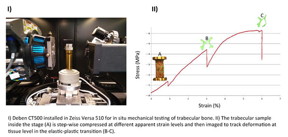
Woolpit, UK | Posted on June 13th, 2017The Zeiss Global Centre (ZGC) is a strategic collaboration between the School of Engineering at the University of Portsmouth and Carl Zeiss Ltd. The Centre is directed by Professor Asa Barber (bio-inspired engineering) and Dr Gianluca Tozzi (healthcare applications). They will lead research into the structural competence of biological structures, biomaterials and bio-inspired engineering materials, through advanced X-ray microscopy. The ZGC is equipped with the latest x-ray imaging and in-situ mechanical testing technology, as well as high-performance computing facilities and dedicated, licensed software for accurate post-processing and analysis of images.
Dr Tozzi describes his research and how he came to choose the µXCT stages from Deben: “Our aim is to produce world-leading research by combining high-resolution imaging, in situ mechanics and Digital Volume Correlation (DVC) to explore the behaviour of biological tissues and bio-inspired structures. The ZGC is equipped with two Zeiss systems for x-ray microscopy (Versa 520 and Versa 510), capable of hosting our Deben in situ mechanical stages: the CT5000 and CT500. These provide a clear interpretation of how the properties of materials change under different loading conditions, particularly when coupled with innovative techniques such as DVC.”
Environmental control is vital to the work of Dr Tozzi and his colleagues: “Our Deben loading stages are very versatile in terms of load capacity and in addition they provide the possibility to test our samples in simulated physiological environment (i.e. liquid chamber and temperature control). This is extremely important for our applications, as often we have to deal with biological tissue mechanics that requires appropriate environmental conditions. We were actually one of the first Universities in the country to adopt Deben rigs for our research. Our first 3kN custom-made loading stage (still in use) was commissioned in 2010 and we have recently taken delivery of our latest unit (CT500).”
The Deben Microtest CT tensile stages for µXCT systems allow samples to be examined using customised load cells in the range from 150 N up to 5000 N (5 kN). The compact design of these testing stages allow them to be used with the smallest high resolution µXCT systems providing a range of tensile and compression stages with forces up to 20 kN and resolutions down to 25 mN. Systems are controlled from the comprehensive MICROTEST tensile stage control software giving a wide range of control functions and a live display of load verses extension and supplied with all required cabling and mounting adaptors for users’ µXCT systems. Custom versions are available with Peltier heating & cooling from -20 °C to +160 °C, extended stroke and travel. To obtain full details of the Deben applications and product portfolio, please visit www.deben.co.uk.
####
About Deben
Deben are a UK precision engineering company specialising in the field of in-situ tensile testing, motion control and specimen cooling for microscopy applications. Established in 1986 and named after a Suffolk river, Deben now operate from a large, modern business unit in Woolpit near Bury St. Edmunds in Suffolk. The product groups are motor control systems, in-situ micro-tensile stages, Peltier heating & cooling stages, detectors for SEMs and electro-static beam blankers. The company also makes custom and OEM versions of these products to specifically meet customer requirements.
Deben provide consultancy, design and prototype manufacturing services. In house facilities include SolidWorks and SolidEdge 3D CAD and COSMOS finite element analysis software, CNC machining, electronics design and manufacture and software design using Visual C++, Microsoft.net and DirectX. Utilising these resources and experience, Deben manufacture products for OEMs and end users in the UK and overseas.
Deben UK Ltd. is a subsidiary company of UK based Judges Scientific plc.
For more information, please click here
Contacts:
Deben UK Limited
Brickfields Business Park
Old Stowmarket Road
Woolpit, Bury St Edmunds
Suffolk IP30 9QS, UK
T +44 (0)1359 244870
www.deben.co.uk
Talking Science Limited
39 de Bohun Court
Saffron Walden
Essex CB10 2BA
T +44(0)1799 521881
M +44(0)7843 012997
www.talking-science.com
Copyright © Deben
If you have a comment, please Contact us.Issuers of news releases, not 7th Wave, Inc. or Nanotechnology Now, are solely responsible for the accuracy of the content.
Bookmark:


| Related News Press |
News and information
![]() Quantum computer improves AI predictions April 17th, 2026
Quantum computer improves AI predictions April 17th, 2026
![]() Flexible sensor gains sensitivity under pressure April 17th, 2026
Flexible sensor gains sensitivity under pressure April 17th, 2026
![]() A reusable chip for particulate matter sensing April 17th, 2026
A reusable chip for particulate matter sensing April 17th, 2026
![]() Detecting vibrational quantum beating in the predissociation dynamics of SF6 using time-resolved photoelectron spectroscopy April 17th, 2026
Detecting vibrational quantum beating in the predissociation dynamics of SF6 using time-resolved photoelectron spectroscopy April 17th, 2026
Imaging
![]() Simple algorithm paired with standard imaging tool could predict failure in lithium metal batteries August 8th, 2025
Simple algorithm paired with standard imaging tool could predict failure in lithium metal batteries August 8th, 2025
Discoveries
![]() Quantum computer improves AI predictions April 17th, 2026
Quantum computer improves AI predictions April 17th, 2026
![]() Flexible sensor gains sensitivity under pressure April 17th, 2026
Flexible sensor gains sensitivity under pressure April 17th, 2026
![]() A reusable chip for particulate matter sensing April 17th, 2026
A reusable chip for particulate matter sensing April 17th, 2026
![]() Detecting vibrational quantum beating in the predissociation dynamics of SF6 using time-resolved photoelectron spectroscopy April 17th, 2026
Detecting vibrational quantum beating in the predissociation dynamics of SF6 using time-resolved photoelectron spectroscopy April 17th, 2026
Announcements
![]() A fundamentally new therapeutic approach to cystic fibrosis: Nanobody repairs cellular defect April 17th, 2026
A fundamentally new therapeutic approach to cystic fibrosis: Nanobody repairs cellular defect April 17th, 2026
![]() UC Irvine physicists discover method to reverse ‘quantum scrambling’ : The work addresses the problem of information loss in quantum computing system April 17th, 2026
UC Irvine physicists discover method to reverse ‘quantum scrambling’ : The work addresses the problem of information loss in quantum computing system April 17th, 2026
Tools
![]() Metasurfaces smooth light to boost magnetic sensing precision January 30th, 2026
Metasurfaces smooth light to boost magnetic sensing precision January 30th, 2026
![]() From sensors to smart systems: the rise of AI-driven photonic noses January 30th, 2026
From sensors to smart systems: the rise of AI-driven photonic noses January 30th, 2026
![]() Japan launches fully domestically produced quantum computer: Expo visitors to experience quantum computing firsthand August 8th, 2025
Japan launches fully domestically produced quantum computer: Expo visitors to experience quantum computing firsthand August 8th, 2025
|
|
||
|
|
||
| The latest news from around the world, FREE | ||
|
|
||
|
|
||
| Premium Products | ||
|
|
||
|
Only the news you want to read!
Learn More |
||
|
|
||
|
Full-service, expert consulting
Learn More |
||
|
|
||