Home > Press > BASF and Fraunhofer IPMS-CNT jointly develop electronic materials
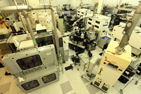 |
| Clean room at Fraunhofer IPMS-CNT Dresden. |
Abstract:
BASF and Fraunhofer IPMS-CNT announced today that they have joined forces to develop innovative solutions for the semiconductor industry. BASF has installed a modern tool for electrochemical metal deposition at the Fraunhofer IPMS Center for Nanoelectronic Technologies (CNT) in Dresden.
BASF and Fraunhofer IPMS-CNT jointly develop electronic materials
Ludwigshafen, Dresden | Posted on June 30th, 2015In pilot tests at the CNT, the latest technologies and innovative chemicals are further developed and tailored for BASF customers. BASF and Fraunhofer are using the same tool and technology used by customers, enabling customers to significantly reduce qualification effort. This saves customers development time, reduces their costs, and allows them to work more efficiently. When the pilot tests at the CNT are completed, customers will have direct access to ready-to-use processes for the production of advanced electronic materials.
"The collaboration with Fraunhofer IPMS-CNT in Dresden is further proof of BASF's commitment to meet the growing demands of the semiconductor industry. It allows our global customers to evaluate our innovative solutions for advanced microchip technologies under production conditions�, says Dr. Lothar Laupichler, Senior Vice President, Electronic Materials at BASF. "In our global R&D network, which now includes IPMS-CNT, we will be collaborating with customers to develop products for the semiconductor industry that surpass current standards."
Dr. Romy Liske, business unit manager at the Fraunhofer Center for Nanoelectronic Technologies, adds, "The further development of materials and processes together with BASF is an important step toward achieving the ever-growing requirements that microchips have to fulfill in terms of functionality, speed, and energy efficiency."
Microchips are widely used in the electronics industry, for example in computers, mobile phones, and electronic components for automobiles. They are manufactured on monocrystalline silicon wafers typically 300 mm in diameter in extremely clean environments known as clean rooms. The network of conductor paths in a microchip is created by means of electrochemical deposition.
####
About BASF
At BASF, we create chemistry � and have been doing so for 150 years. Our portfolio ranges from chemicals, plastics, performance products and crop protection products to oil and gas. As the world's leading chemical company, we combine economic success with environmental protection and social responsibility. Through science and innovation, we enable our customers in nearly every industry to meet the current and future needs of society. Our products and solutions contribute to conserving resources, ensuring nutrition and improving quality of life. We have summed up this contribution in our corporate purpose: "We create chemistry for a sustainable future." BASF posted sales of around �74 billion in 2014 and at the year end employed a workforce of more than 113,000 people. BASF is listed on the stock markets in Frankfurt (BAS), London (BFA), and Zurich (AN). Further information on BASF is available on the Internet at www.basf.com.
About Fraunhofer IPMS � Center Nanoelectronic Technologies (IPMS-CNT)
The Fraunhofer Gesellschaft is the largest organization for applied research in Europe with 23,000 employees. Fraunhofer IPMS is one of 67 institutes in Germany and exemplifies the close partnership between applied research and semiconductor production facilities in the industrial location "Silicon Saxony". At the Center Nanoelectronic Technologies (CNT), Fraunhofer IPMS carries out applied research on 300mm silicon wafers for microchip manufacturers, component suppliers, and R&D partners. The services available at IPMS-CNT include the process modules of nanopatterning, high-k devices, interconnects / Cu metallization and sub-nm characterization. The wide- ranging expertise and industry standard mean that developments and new processes can be integrated quickly and without risk in the customers' processes, minimizing production costs and saving time. www.ipms.fraunhofer.de
For more information, please click here
Contacts:
BASF Global
Andrew Sung
Communications Manager Electronic Materials
Phone: +82 (0)2 6395 7625
BASF Europe
Jörg Kordes
Communications Monomers
Phone: +49 (0) 621 60-43776
Fraunhofer IPMS
Peter Felten
Business Development & Strategy
Center Nanoelectronic Technologies (CNT)
Phone: +49 351 2607-3046
Copyright © BASF
If you have a comment, please Contact us.Issuers of news releases, not 7th Wave, Inc. or Nanotechnology Now, are solely responsible for the accuracy of the content.
Bookmark:


| Related News Press |
News and information
![]() Quantum computer improves AI predictions April 17th, 2026
Quantum computer improves AI predictions April 17th, 2026
![]() Flexible sensor gains sensitivity under pressure April 17th, 2026
Flexible sensor gains sensitivity under pressure April 17th, 2026
![]() A reusable chip for particulate matter sensing April 17th, 2026
A reusable chip for particulate matter sensing April 17th, 2026
![]() Detecting vibrational quantum beating in the predissociation dynamics of SF6 using time-resolved photoelectron spectroscopy April 17th, 2026
Detecting vibrational quantum beating in the predissociation dynamics of SF6 using time-resolved photoelectron spectroscopy April 17th, 2026
Chip Technology
![]() A reusable chip for particulate matter sensing April 17th, 2026
A reusable chip for particulate matter sensing April 17th, 2026
![]() Metasurfaces smooth light to boost magnetic sensing precision January 30th, 2026
Metasurfaces smooth light to boost magnetic sensing precision January 30th, 2026
Materials/Metamaterials/Magnetoresistance
![]() First real-time observation of two-dimensional melting process: Researchers at Mainz University unveil new insights into magnetic vortex structures August 8th, 2025
First real-time observation of two-dimensional melting process: Researchers at Mainz University unveil new insights into magnetic vortex structures August 8th, 2025
![]() Researchers unveil a groundbreaking clay-based solution to capture carbon dioxide and combat climate change June 6th, 2025
Researchers unveil a groundbreaking clay-based solution to capture carbon dioxide and combat climate change June 6th, 2025
![]() A 1960s idea inspires NBI researchers to study hitherto inaccessible quantum states June 6th, 2025
A 1960s idea inspires NBI researchers to study hitherto inaccessible quantum states June 6th, 2025
![]() Institute for Nanoscience hosts annual proposal planning meeting May 16th, 2025
Institute for Nanoscience hosts annual proposal planning meeting May 16th, 2025
Announcements
![]() A fundamentally new therapeutic approach to cystic fibrosis: Nanobody repairs cellular defect April 17th, 2026
A fundamentally new therapeutic approach to cystic fibrosis: Nanobody repairs cellular defect April 17th, 2026
![]() UC Irvine physicists discover method to reverse �quantum scrambling� : The work addresses the problem of information loss in quantum computing system April 17th, 2026
UC Irvine physicists discover method to reverse �quantum scrambling� : The work addresses the problem of information loss in quantum computing system April 17th, 2026
|
|
||
|
|
||
| The latest news from around the world, FREE | ||
|
|
||
|
|
||
| Premium Products | ||
|
|
||
|
Only the news you want to read!
Learn More |
||
|
|
||
|
Full-service, expert consulting
Learn More |
||
|
|
||