Home > Press > Scientists craft atomically seamless, thinnest-possible semiconductor junctions
 |
| U of Washington
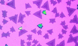
As seen under an optical microscope, the heterostructures have a triangular shape. The two different monolayer semiconductors can be recognized through their different colors. |
Abstract:
Scientists have developed what they believe is the thinnest-possible semiconductor, a new class of nanoscale materials made in sheets only three atoms thick.
Scientists craft atomically seamless, thinnest-possible semiconductor junctions
Seattle, WA | Posted on August 26th, 2014The University of Washington researchers have demonstrated that two of these single-layer semiconductor materials can be connected in an atomically seamless fashion known as a heterojunction. This result could be the basis for next-generation flexible and transparent computing, better light-emitting diodes, or LEDs, and solar technologies.
"Heterojunctions are fundamental elements of electronic and photonic devices," said senior author Xiaodong Xu, a UW assistant professor of materials science and engineering and of physics. "Our experimental demonstration of such junctions between two-dimensional materials should enable new kinds of transistors, LEDs, nanolasers, and solar cells to be developed for highly integrated electronic and optical circuits within a single atomic plane."
The research was published online this week in Nature Materials.
The researchers discovered that two flat semiconductor materials can be connected edge-to-edge with crystalline perfection. They worked with two single-layer, or monolayer, materials - molybdenum diselenide and tungsten diselenide - that have very similar structures, which was key to creating the composite two-dimensional semiconductor.
Collaborators from the electron microscopy center at the University of Warwick in England found that all the atoms in both materials formed a single honeycomb lattice structure, without any distortions or discontinuities. This provides the strongest possible link between two single-layer materials, necessary for flexible devices. Within the same family of materials it is feasible that researchers could bond other pairs together in the same way.
The researchers created the junctions in a small furnace at the UW. First, they inserted a powder mixture of the two materials into a chamber heated to 900 degrees Celsius (1,652 F). Hydrogen gas was then passed through the chamber and the evaporated atoms from one of the materials were carried toward a cooler region of the tube and deposited as single-layer crystals in the shape of triangles.
After a while, evaporated atoms from the second material then attached to the edges of the triangle to create a seamless semiconducting heterojunction.
"This is a scalable technique," said Sanfeng Wu, a UW doctoral student in physics and one of the lead authors. "Because the materials have different properties, they evaporate and separate at different times automatically. The second material forms around the first triangle that just previously formed. That's why these lattices are so beautifully connected."
With a larger furnace, it would be possible to mass-produce sheets of these semiconductor heterostructures, the researchers said. On a small scale, it takes about five minutes to grow the crystals, with up to two hours of heating and cooling time.
"We are very excited about the new science and engineering opportunities provided by these novel structures," said senior author David Cobden, a UW professor of physics. "In the future, combinations of two-dimensional materials may be integrated together in this way to form all kinds of interesting electronic structures such as in-plane quantum wells and quantum wires, superlattices, fully functioning transistors, and even complete electronic circuits."
The researchers have already demonstrated that the junction interacts with light much more strongly than the rest of the monolayer, which is encouraging for optoelectric and photonic applications like solar cells.
Other co-authors are Chunming Huang and Pasqual Rivera of UW physics; Ana Sanchez, Richard Beanland and Jonathan Peters at the University of Warwick; Jason Ross of UW materials science and engineering; and Wang Yao, a theoretical physicist of the University of Hong Kong.
This research was funded by the U.S. Department of Energy, the UW's Clean Energy Institute, the Research Grant Council of Hong Kong, the University Grants Committee of Hong Kong, the Croucher Foundation, the Science City Research Alliance and the Higher Education Funding Council for England's Strategic Development Fund.
Grant numbers: U.S. Department of Energy, Basic Energy Sciences, Materials Sciences and Engineering Division (DE-SC0008145) (DE-SC0002197).
####
For more information, please click here
Contacts:
Michelle Ma
206-543-2580
Sanfeng Wu
Copyright © University of Washington
If you have a comment, please Contact us.Issuers of news releases, not 7th Wave, Inc. or Nanotechnology Now, are solely responsible for the accuracy of the content.
Bookmark:


| Related News Press |
News and information
![]() Quantum computer improves AI predictions April 17th, 2026
Quantum computer improves AI predictions April 17th, 2026
![]() Flexible sensor gains sensitivity under pressure April 17th, 2026
Flexible sensor gains sensitivity under pressure April 17th, 2026
![]() A reusable chip for particulate matter sensing April 17th, 2026
A reusable chip for particulate matter sensing April 17th, 2026
![]() Detecting vibrational quantum beating in the predissociation dynamics of SF6 using time-resolved photoelectron spectroscopy April 17th, 2026
Detecting vibrational quantum beating in the predissociation dynamics of SF6 using time-resolved photoelectron spectroscopy April 17th, 2026
Imaging
![]() Simple algorithm paired with standard imaging tool could predict failure in lithium metal batteries August 8th, 2025
Simple algorithm paired with standard imaging tool could predict failure in lithium metal batteries August 8th, 2025
Govt.-Legislation/Regulation/Funding/Policy
![]() Quantum computer improves AI predictions April 17th, 2026
Quantum computer improves AI predictions April 17th, 2026
![]() Metasurfaces smooth light to boost magnetic sensing precision January 30th, 2026
Metasurfaces smooth light to boost magnetic sensing precision January 30th, 2026
![]() New imaging approach transforms study of bacterial biofilms August 8th, 2025
New imaging approach transforms study of bacterial biofilms August 8th, 2025
Chip Technology
![]() A reusable chip for particulate matter sensing April 17th, 2026
A reusable chip for particulate matter sensing April 17th, 2026
![]() Metasurfaces smooth light to boost magnetic sensing precision January 30th, 2026
Metasurfaces smooth light to boost magnetic sensing precision January 30th, 2026
Discoveries
![]() Quantum computer improves AI predictions April 17th, 2026
Quantum computer improves AI predictions April 17th, 2026
![]() Flexible sensor gains sensitivity under pressure April 17th, 2026
Flexible sensor gains sensitivity under pressure April 17th, 2026
![]() A reusable chip for particulate matter sensing April 17th, 2026
A reusable chip for particulate matter sensing April 17th, 2026
![]() Detecting vibrational quantum beating in the predissociation dynamics of SF6 using time-resolved photoelectron spectroscopy April 17th, 2026
Detecting vibrational quantum beating in the predissociation dynamics of SF6 using time-resolved photoelectron spectroscopy April 17th, 2026
Announcements
![]() A fundamentally new therapeutic approach to cystic fibrosis: Nanobody repairs cellular defect April 17th, 2026
A fundamentally new therapeutic approach to cystic fibrosis: Nanobody repairs cellular defect April 17th, 2026
![]() UC Irvine physicists discover method to reverse �quantum scrambling� : The work addresses the problem of information loss in quantum computing system April 17th, 2026
UC Irvine physicists discover method to reverse �quantum scrambling� : The work addresses the problem of information loss in quantum computing system April 17th, 2026
Interviews/Book Reviews/Essays/Reports/Podcasts/Journals/White papers/Posters
![]() A fundamentally new therapeutic approach to cystic fibrosis: Nanobody repairs cellular defect April 17th, 2026
A fundamentally new therapeutic approach to cystic fibrosis: Nanobody repairs cellular defect April 17th, 2026
![]() UC Irvine physicists discover method to reverse �quantum scrambling� : The work addresses the problem of information loss in quantum computing system April 17th, 2026
UC Irvine physicists discover method to reverse �quantum scrambling� : The work addresses the problem of information loss in quantum computing system April 17th, 2026
Tools
![]() Metasurfaces smooth light to boost magnetic sensing precision January 30th, 2026
Metasurfaces smooth light to boost magnetic sensing precision January 30th, 2026
![]() From sensors to smart systems: the rise of AI-driven photonic noses January 30th, 2026
From sensors to smart systems: the rise of AI-driven photonic noses January 30th, 2026
![]() Japan launches fully domestically produced quantum computer: Expo visitors to experience quantum computing firsthand August 8th, 2025
Japan launches fully domestically produced quantum computer: Expo visitors to experience quantum computing firsthand August 8th, 2025
Research partnerships
![]() Lab to industry: InSe wafer-scale breakthrough for future electronics August 8th, 2025
Lab to industry: InSe wafer-scale breakthrough for future electronics August 8th, 2025
![]() HKU physicists uncover hidden order in the quantum world through deconfined quantum critical points April 25th, 2025
HKU physicists uncover hidden order in the quantum world through deconfined quantum critical points April 25th, 2025
|
|
||
|
|
||
| The latest news from around the world, FREE | ||
|
|
||
|
|
||
| Premium Products | ||
|
|
||
|
Only the news you want to read!
Learn More |
||
|
|
||
|
Full-service, expert consulting
Learn More |
||
|
|
||