Home > Press > Nanometer-scale diamond tips improve nano-manufacturing
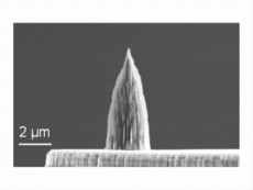 |
| Diamond nano-tip integrated onto the micro-heater of a doped silicon microcantilever. The tip has a radius of 10 nm. |
Abstract:
One of the most promising innovations of nanotechnology has been the ability to perform rapid nanofabrication using nanometer-scale tips. The fabrication speed can be dramatically increased by using heat. High speed and high temperature have been known to degrade the tip… until now.
Nanometer-scale diamond tips improve nano-manufacturing
Urbana, IL | Posted on November 14th, 2012"Thermal processing is widely used in manufacturing," according to William King, the College of Engineering Bliss Professor at Illinois. "We have been working to shrink thermal processing to the nanometer scale, where we can use a nanometer-scale heat source to add or remove material, or induce a physical or chemical reaction."
One of the key challenges has been the reliability of the nanometer-scale tips, especially with performing nano-writing on hard, semiconductor surfaces. Now, researchers at the University of Illinois, University of Pennsylvania, and Advanced Diamond Technologies Inc., have created a new type of nano-tip for thermal processing, which is made entirely out of diamond.
"The end of the diamond tip is 10 nm in size," King explained. "Not only can the tip be used for nanometer-scale thermal processing, but it is extremely resistant to wear."
The research findings are reported in the article, "Ultrananocrystalline diamond tip integrated onto a heated atomic force microscope (AFM) cantilever," that appears in in the journal Nanotechnology. The study shows how the 10 nm diamond tip scans in contact with a surface for a distance of more than 1.2 meters, and experiences essentially no wear over that distance.
William King
"The scan distance is equal to 100 million times the size of the tip," said King. "That's the equivalent of a person walking around the circumference of the earth four times, and doing so with no measurable wear."
"The robustness of these diamond-based probes under such harsh conditions—high temperatures and stresses in an oxidizing environment—is quite remarkable and exceeds anything I've seen with other AFM probes," said Robert Carpick, professor of mechanical engineering and applied mechanics at University of Pennsylvania and co-author on the study. "This level of durability combined with the multifunctionality of a thermal probe really opens up new applications for the AFM."
"We are pleased with the results since they prove once again the superiority of diamond tips to any other types of probe tips when it comes to low wear and resistance to harsh environment," said Nicolaie Moldovan, a scientist at Advanced Diamond Technologies and co-author on the study.
The authors on the study are Hoe-Joon Kim, Suhas Somnath, Jonathan Felts, and William King, University of Illinois; Tevis Jacobs and Robert Carpick, University of Pennsylvania; and Nicolaie Moldovan and John Carlisle, Advanced Diamond Technologies Inc.
####
For more information, please click here
Contacts:
William P. King
217-244-3864
Rick Kubetz
editor
Engineering Communications Office
University of Illinois at Urbana-Champaign
217/244-7716
Copyright © University of Illinois College of Engineering
If you have a comment, please Contact us.Issuers of news releases, not 7th Wave, Inc. or Nanotechnology Now, are solely responsible for the accuracy of the content.
Bookmark:


| Related Links |
| Related News Press |
News and information
![]() Quantum computer improves AI predictions April 17th, 2026
Quantum computer improves AI predictions April 17th, 2026
![]() Flexible sensor gains sensitivity under pressure April 17th, 2026
Flexible sensor gains sensitivity under pressure April 17th, 2026
![]() A reusable chip for particulate matter sensing April 17th, 2026
A reusable chip for particulate matter sensing April 17th, 2026
![]() Detecting vibrational quantum beating in the predissociation dynamics of SF6 using time-resolved photoelectron spectroscopy April 17th, 2026
Detecting vibrational quantum beating in the predissociation dynamics of SF6 using time-resolved photoelectron spectroscopy April 17th, 2026
Imaging
![]() Simple algorithm paired with standard imaging tool could predict failure in lithium metal batteries August 8th, 2025
Simple algorithm paired with standard imaging tool could predict failure in lithium metal batteries August 8th, 2025
Discoveries
![]() Quantum computer improves AI predictions April 17th, 2026
Quantum computer improves AI predictions April 17th, 2026
![]() Flexible sensor gains sensitivity under pressure April 17th, 2026
Flexible sensor gains sensitivity under pressure April 17th, 2026
![]() A reusable chip for particulate matter sensing April 17th, 2026
A reusable chip for particulate matter sensing April 17th, 2026
![]() Detecting vibrational quantum beating in the predissociation dynamics of SF6 using time-resolved photoelectron spectroscopy April 17th, 2026
Detecting vibrational quantum beating in the predissociation dynamics of SF6 using time-resolved photoelectron spectroscopy April 17th, 2026
Announcements
![]() A fundamentally new therapeutic approach to cystic fibrosis: Nanobody repairs cellular defect April 17th, 2026
A fundamentally new therapeutic approach to cystic fibrosis: Nanobody repairs cellular defect April 17th, 2026
![]() UC Irvine physicists discover method to reverse ‘quantum scrambling’ : The work addresses the problem of information loss in quantum computing system April 17th, 2026
UC Irvine physicists discover method to reverse ‘quantum scrambling’ : The work addresses the problem of information loss in quantum computing system April 17th, 2026
Tools
![]() Metasurfaces smooth light to boost magnetic sensing precision January 30th, 2026
Metasurfaces smooth light to boost magnetic sensing precision January 30th, 2026
![]() From sensors to smart systems: the rise of AI-driven photonic noses January 30th, 2026
From sensors to smart systems: the rise of AI-driven photonic noses January 30th, 2026
![]() Japan launches fully domestically produced quantum computer: Expo visitors to experience quantum computing firsthand August 8th, 2025
Japan launches fully domestically produced quantum computer: Expo visitors to experience quantum computing firsthand August 8th, 2025
|
|
||
|
|
||
| The latest news from around the world, FREE | ||
|
|
||
|
|
||
| Premium Products | ||
|
|
||
|
Only the news you want to read!
Learn More |
||
|
|
||
|
Full-service, expert consulting
Learn More |
||
|
|
||