Home > Press > One-molecule-thick material has big advantages: MIT researchers produce complex electronic circuits from molybdenum disulfide, a material that could have many more applications
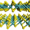 |
| Diagram shows the flat-sheet structure of the material used by the MIT team, molybdenum disulfide. Molybdenum atoms are shown in teal, and sulfur atoms in yellow. Image courtesy of Wang et al. |
Abstract:
The discovery of graphene, a material just one atom thick and possessing exceptional strength and other novel properties, started an avalanche of research around its use for everything from electronics to optics to structural materials. But new research suggests that was just the beginning: A whole family of two-dimensional materials may open up even broader possibilities for applications that could change many aspects of modern life.
One-molecule-thick material has big advantages: MIT researchers produce complex electronic circuits from molybdenum disulfide, a material that could have many more applications
Cambridge, MA | Posted on August 23rd, 2012The latest "new" material, molybdenum disulfide (MoS2) � which has actually been used for decades, but not in its 2-D form � was first described just a year ago by researchers in Switzerland. But in that year, researchers at MIT � who struggled for several years to build electronic circuits out of graphene with very limited results (except for radio-frequency applications) � have already succeeded in making a variety of electronic components from MoS2. They say the material could help usher in radically new products, from whole walls that glow to clothing with embedded electronics to glasses with built-in display screens.
A report on the production of complex electronic circuits from the new material was published online this month in the journal Nano Letters; the paper is authored by Han Wang and Lili Yu, graduate students in the Department of Electrical Engineering and Computer Science (EECS); Tom�s Palacios, the Emmanuel E. Landsman Associate Professor of EECS; and others at MIT and elsewhere.
Palacios says he thinks graphene and MoS2 are just the beginning of a new realm of research on two-dimensional materials. "It's the most exciting time for electronics in the last 20 or 30 years," he says. "It's opening up the door to a completely new domain of electronic materials and devices."
Like graphene, itself a 2-D form of graphite, molybdenum disulfide has been used for many years as an industrial lubricant. But it had never been seen as a 2-D platform for electronic devices until last year, when scientists at the Swiss university EPFL produced a transistor on the material.
MIT researchers quickly swung into action: Yi-Hsien Lee, a postdoc in associate professor Jing Kong's group in EECS, found a good way to make large sheets of the material using a chemical vapor deposition process. Lee came up with this method while working with Lain-Jong Li at Academia Sinica in Taiwan and improved it after coming to MIT. Palacios, Wang and Yu then set to producing building blocks of electronic circuits on the sheets made by Lee, as well as on MoS2 flakes produced by a mechanical method, which were used for the work described in the new paper.
Wang had been struggling to build circuits on graphene for his doctoral thesis research, but found it much easier to do with the new material. There was a "hefty bottleneck" to making progress with graphene, he explains, because that material lacks a bandgap � the key property that makes it possible to create transistors, the basic component of logic and memory circuits. While graphene needs to be modified in exacting ways in order to create a bandgap, MoS2 just naturally comes with one.
The lack of a bandgap, Wang explains, means that with a switch made of graphene, "you can turn it on, but you can't turn it off. That means you can't do digital logic." So people have for years been searching for a material that shares some of graphene's extraordinary properties, but also has this missing quality � as molybdenum disulfide does.
Because it already is widely produced as a lubricant, and thanks to ongoing work at MIT and other labs on making it into large sheets, scaling up production of the material for practical uses should be much easier than with other new materials, Wang and Palacios say.
Wang and Palacios were able to fabricate a variety of basic electronic devices on the material: an inverter, which switches an input voltage to its opposite; a NAND gate, a basic logic element that can be combined to carry out almost any kind of logic operation; a memory device, one of the key components of all computational devices; and a more complex circuit called a ring oscillator, made up of 12 interconnected transistors, which can produce a precisely tuned wave output.
Palacios says one potential application of the new material is large-screen displays such as television sets and computer monitors, where a separate transistor controls each pixel of the display. Because the material is just one molecule thick � unlike the highly purified silicon that is used for conventional transistors and must be millions of atoms thick � even a very large display would use only an infinitesimal quantity of the raw materials. This could potentially reduce cost and weight and improve energy efficiency.
In the future, it could also enable entirely new kinds of devices. The material could be used, in combination with other 2-D materials, to make light-emitting devices. Instead of producing a point source of light from one bulb, an entire wall could be made to glow, producing softer, less glaring light. Similarly, the antenna and other circuitry of a cellphone might be woven into fabric, providing a much more sensitive antenna that needs less power and could be incorporated into clothing, Palacios says.
The material is so thin that it's completely transparent, and it can be deposited on virtually any other material. For example, MoS2 could be applied to glass, producing displays built into a pair of eyeglasses or the window of a house or office.
Ali Javey, an associate professor of electrical engineering and computer science at the University of California at Berkeley, who was not involved in this research, says layered materials such as MoS2 are "a promising class of materials for future electronics," but cautions that "the future looks bright for layered semiconductors, but still work needs to be done to better understand their performance limits and large-scale manufacturing."
Overall, Javey says, the MIT team's research is "elegant" work that "takes an important step forward in advancing the field of layered semiconductors."
In addition to Palacios, Kong, Wang, Yu and Lee, the work was carried out by graduate student Allen Hsu and MIT affiliate Yumeng Shi, with U.S. Army Research Laboratory researchers Matthew Chin and Madan Dubey, and Lain-Jong Li of Academia Sinica in Taiwan. The work was funded by the U.S. Office of Naval Research, the Microelectronics Advanced Research Corporation Focus Center for Materials, the National Science Foundation and the Army Research Laboratory.
Written by: David L. Chandler, MIT News Office
####
For more information, please click here
Contacts:
Sarah McDonnell
MIT News Office
617-253-8923
Copyright © MIT
If you have a comment, please Contact us.Issuers of news releases, not 7th Wave, Inc. or Nanotechnology Now, are solely responsible for the accuracy of the content.
Bookmark:


| Related Links |
![]() Paper: "Integrated Circuits Based on Bilayer MoS2 Transistors":
Paper: "Integrated Circuits Based on Bilayer MoS2 Transistors":
![]() Paper: "Synthesis of Large-Area MoS2 Atomic Layers with Chemical Vapor Deposition":
Paper: "Synthesis of Large-Area MoS2 Atomic Layers with Chemical Vapor Deposition":
![]() MIT Center for Graphene Devices and Systems:
MIT Center for Graphene Devices and Systems:
![]() Department of Electrical Engineering and Computer Science:
Department of Electrical Engineering and Computer Science:
![]() Microsystems Technology Laboratory:
Microsystems Technology Laboratory:
![]() ARCHIVE: "Explained: Bandgap":
ARCHIVE: "Explained: Bandgap":
![]() From the MIT Energy Initiative: �Improving the transistor: Small device, big energy savings�:
From the MIT Energy Initiative: �Improving the transistor: Small device, big energy savings�:
| Related News Press |
News and information
![]() Quantum computer improves AI predictions April 17th, 2026
Quantum computer improves AI predictions April 17th, 2026
![]() Flexible sensor gains sensitivity under pressure April 17th, 2026
Flexible sensor gains sensitivity under pressure April 17th, 2026
![]() A reusable chip for particulate matter sensing April 17th, 2026
A reusable chip for particulate matter sensing April 17th, 2026
![]() Detecting vibrational quantum beating in the predissociation dynamics of SF6 using time-resolved photoelectron spectroscopy April 17th, 2026
Detecting vibrational quantum beating in the predissociation dynamics of SF6 using time-resolved photoelectron spectroscopy April 17th, 2026
Display technology/LEDs/SS Lighting/OLEDs
![]() Spinel-type sulfide semiconductors to operate the next-generation LEDs and solar cells For solar-cell absorbers and green-LED source October 3rd, 2025
Spinel-type sulfide semiconductors to operate the next-generation LEDs and solar cells For solar-cell absorbers and green-LED source October 3rd, 2025
Graphene/ Graphite
![]() Electrifying results shed light on graphene foam as a potential material for lab grown cartilage June 6th, 2025
Electrifying results shed light on graphene foam as a potential material for lab grown cartilage June 6th, 2025
![]() Breakthrough in proton barrier films using pore-free graphene oxide: Kumamoto University researchers achieve new milestone in advanced coating technologies September 13th, 2024
Breakthrough in proton barrier films using pore-free graphene oxide: Kumamoto University researchers achieve new milestone in advanced coating technologies September 13th, 2024
Govt.-Legislation/Regulation/Funding/Policy
![]() Quantum computer improves AI predictions April 17th, 2026
Quantum computer improves AI predictions April 17th, 2026
![]() Metasurfaces smooth light to boost magnetic sensing precision January 30th, 2026
Metasurfaces smooth light to boost magnetic sensing precision January 30th, 2026
![]() New imaging approach transforms study of bacterial biofilms August 8th, 2025
New imaging approach transforms study of bacterial biofilms August 8th, 2025
Possible Futures
![]() A fundamentally new therapeutic approach to cystic fibrosis: Nanobody repairs cellular defect April 17th, 2026
A fundamentally new therapeutic approach to cystic fibrosis: Nanobody repairs cellular defect April 17th, 2026
![]() UC Irvine physicists discover method to reverse �quantum scrambling� : The work addresses the problem of information loss in quantum computing system April 17th, 2026
UC Irvine physicists discover method to reverse �quantum scrambling� : The work addresses the problem of information loss in quantum computing system April 17th, 2026
Chip Technology
![]() A reusable chip for particulate matter sensing April 17th, 2026
A reusable chip for particulate matter sensing April 17th, 2026
![]() Metasurfaces smooth light to boost magnetic sensing precision January 30th, 2026
Metasurfaces smooth light to boost magnetic sensing precision January 30th, 2026
Discoveries
![]() Quantum computer improves AI predictions April 17th, 2026
Quantum computer improves AI predictions April 17th, 2026
![]() Flexible sensor gains sensitivity under pressure April 17th, 2026
Flexible sensor gains sensitivity under pressure April 17th, 2026
![]() A reusable chip for particulate matter sensing April 17th, 2026
A reusable chip for particulate matter sensing April 17th, 2026
![]() Detecting vibrational quantum beating in the predissociation dynamics of SF6 using time-resolved photoelectron spectroscopy April 17th, 2026
Detecting vibrational quantum beating in the predissociation dynamics of SF6 using time-resolved photoelectron spectroscopy April 17th, 2026
Materials/Metamaterials/Magnetoresistance
![]() First real-time observation of two-dimensional melting process: Researchers at Mainz University unveil new insights into magnetic vortex structures August 8th, 2025
First real-time observation of two-dimensional melting process: Researchers at Mainz University unveil new insights into magnetic vortex structures August 8th, 2025
![]() Researchers unveil a groundbreaking clay-based solution to capture carbon dioxide and combat climate change June 6th, 2025
Researchers unveil a groundbreaking clay-based solution to capture carbon dioxide and combat climate change June 6th, 2025
![]() A 1960s idea inspires NBI researchers to study hitherto inaccessible quantum states June 6th, 2025
A 1960s idea inspires NBI researchers to study hitherto inaccessible quantum states June 6th, 2025
![]() Institute for Nanoscience hosts annual proposal planning meeting May 16th, 2025
Institute for Nanoscience hosts annual proposal planning meeting May 16th, 2025
Announcements
![]() A fundamentally new therapeutic approach to cystic fibrosis: Nanobody repairs cellular defect April 17th, 2026
A fundamentally new therapeutic approach to cystic fibrosis: Nanobody repairs cellular defect April 17th, 2026
![]() UC Irvine physicists discover method to reverse �quantum scrambling� : The work addresses the problem of information loss in quantum computing system April 17th, 2026
UC Irvine physicists discover method to reverse �quantum scrambling� : The work addresses the problem of information loss in quantum computing system April 17th, 2026
Military
![]() Quantum engineers �squeeze� laser frequency combs to make more sensitive gas sensors January 17th, 2025
Quantum engineers �squeeze� laser frequency combs to make more sensitive gas sensors January 17th, 2025
![]() Chainmail-like material could be the future of armor: First 2D mechanically interlocked polymer exhibits exceptional flexibility and strength January 17th, 2025
Chainmail-like material could be the future of armor: First 2D mechanically interlocked polymer exhibits exceptional flexibility and strength January 17th, 2025
![]() Single atoms show their true color July 5th, 2024
Single atoms show their true color July 5th, 2024
![]() NRL charters Navy�s quantum inertial navigation path to reduce drift April 5th, 2024
NRL charters Navy�s quantum inertial navigation path to reduce drift April 5th, 2024
Research partnerships
![]() Lab to industry: InSe wafer-scale breakthrough for future electronics August 8th, 2025
Lab to industry: InSe wafer-scale breakthrough for future electronics August 8th, 2025
![]() HKU physicists uncover hidden order in the quantum world through deconfined quantum critical points April 25th, 2025
HKU physicists uncover hidden order in the quantum world through deconfined quantum critical points April 25th, 2025
|
|
||
|
|
||
| The latest news from around the world, FREE | ||
|
|
||
|
|
||
| Premium Products | ||
|
|
||
|
Only the news you want to read!
Learn More |
||
|
|
||
|
Full-service, expert consulting
Learn More |
||
|
|
||