Home > Press > Cloak and swagger: Engineers use plasmonics to create an invisible photodetector
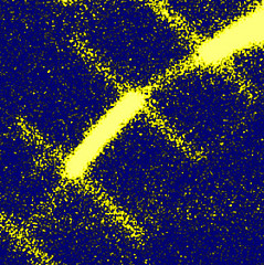 |
| An image showing light scattering from a silicon nanowire running diagonally from bottom left to top right. The brighter areas are bare silicon while the dimmer sections are coated with gold demonstrating how plasmonic cloaking reduces light scattering in the gold-coated sections. Photo: Stanford Nanocharacterization Lab. |
Abstract:
A team of engineers at Stanford and the University of Pennsylvania has for the first time used "plasmonic cloaking" to create a device that can see without being seen - an invisible machine that detects light. It is the first example of what the researchers describe as a new class of devices that controls the flow of light at the nanoscale to produce both optical and electronic functions.
Cloak and swagger: Engineers use plasmonics to create an invisible photodetector
Stanford, CA | Posted on May 21st, 2012It may not be intuitive, but a coating of reflective metal can actually make something less visible, engineers at Stanford and UPenn have shown. They have created an invisible, light-detecting device that can "see without being seen."
At the heart of the device are silicon nanowires covered by a thin cap of gold. By adjusting the ratio of metal to silicon - a technique the engineers refer to as tuning the geometries - they capitalize on favorable nanoscale physics in which the reflected light from the two materials cancel each other to make the device invisible.
Pengyu Fan is the lead author of a paper demonstrating the new device published online May 20th in the journal Nature Photonics. He is a doctoral candidate in materials science and engineering at Stanford University working in Professor Mark Brongersma's group. Brongersma is senior author of the study.
Cloak of invisiblity
Light detection is well known and relatively simple. Silicon generates electrical current when illuminated and is common in solar panels and light sensors today. The Stanford device, however, is a departure in that for the first time it uses a relatively new concept known as plasmonic cloaking to render the device invisible.
The field of plasmonics studies how light interacts with metal nanostructures and induces tiny oscillating electrical currents along the surfaces of the metal and the semiconductor. These currents, in turn, produce scattered light waves.
By carefully designing their device - by tuning the geometries - the engineers have created a plasmonic cloak in which the scattered light from the metal and semiconductor cancel each other perfectly through a phenomenon known as destructive interference.
The rippling light waves in the metal and semiconductor create a separation of positive and negative charges in the materials - a dipole moment, in technical terms. The key is to create a dipole in the gold that is equal in strength but opposite in sign to the dipole in the silicon. When equally strong positive and negative dipoles meet, they cancel each other and the system becomes invisible.
"We found that a carefully engineered gold shell dramatically alters the optical response of the silicon nanowire," said Fan. "Light absorption in the wire drops slightly - by a factor of just four - but the scattering of light drops by 100 times due to the cloaking effect, becoming invisible."
"It seems counterintuitive," said Brongersma, "but you can cover a semiconductor with metal - even one as reflective as gold - and still have the light get through to the silicon. As we show, the metal not only allows the light to reach the silicon where we can detect the current generated, but it makes the wire invisible, too."
Broadly effective
The engineers have shown that plasmonic cloaking is effective across much of the visible spectrum of light and that the effect works regardless of the angle of incoming light or the shape and placement of the metal-covered nanowires in the device. They likewise demonstrate that other metals commonly used in computer chips, like aluminum and copper, work just as well as gold.
To produce invisibility, what matters above all is the tuning of metal and semiconductor.
"If the dipoles do not align properly, the cloaking effect is lessened, or even lost," said Fan. "Having the right amount of materials at the nanoscale, therefore, is key to producing the greatest degree of cloaking."
In the future, the engineers foresee application for such tunable, metal-semiconductor devices in many relevant areas, including solar cells, sensors, solid-state lighting, chip-scale lasers, and more.
In digital cameras and advanced imaging systems, for instance, plasmonically cloaked pixels might reduce the disruptive cross-talk between neighboring pixels that produces blur. It could therefore lead to sharper, more accurate photos and medical images.
"We can even imagine reengineering existing opto-electronic devices to incorporate valuable new functions and to achieve sensor densities not possible today," concluded Brongersma. "There are many emerging opportunities for these photonic building blocks."
Brongersma lab alumnus Professor Linyou Cao and doctoral candidate Farzaneh Afshinmanesh contributed to this research. This work is a collaboration with Professor Nader Engheta and post-doctoral researcher Uday Chettiar from University of Pennsylvania.
By Andrew Myers
Andrew Myers is associate director of communications for the Stanford University School of Engineering.
####
For more information, please click here
Contacts:
Andrew Myers
Associate Director of Communications
650.736.2245
Jamie Beckett
Director of Communications and Alumni Relations
650.736.2241
Copyright © Stanford School of Engineering
If you have a comment, please Contact us.Issuers of news releases, not 7th Wave, Inc. or Nanotechnology Now, are solely responsible for the accuracy of the content.
Bookmark:


| Related News Press |
News and information
![]() Quantum computer improves AI predictions April 17th, 2026
Quantum computer improves AI predictions April 17th, 2026
![]() Flexible sensor gains sensitivity under pressure April 17th, 2026
Flexible sensor gains sensitivity under pressure April 17th, 2026
![]() A reusable chip for particulate matter sensing April 17th, 2026
A reusable chip for particulate matter sensing April 17th, 2026
![]() Detecting vibrational quantum beating in the predissociation dynamics of SF6 using time-resolved photoelectron spectroscopy April 17th, 2026
Detecting vibrational quantum beating in the predissociation dynamics of SF6 using time-resolved photoelectron spectroscopy April 17th, 2026
Imaging
![]() Simple algorithm paired with standard imaging tool could predict failure in lithium metal batteries August 8th, 2025
Simple algorithm paired with standard imaging tool could predict failure in lithium metal batteries August 8th, 2025
![]() First real-time observation of two-dimensional melting process: Researchers at Mainz University unveil new insights into magnetic vortex structures August 8th, 2025
First real-time observation of two-dimensional melting process: Researchers at Mainz University unveil new insights into magnetic vortex structures August 8th, 2025
![]() New imaging approach transforms study of bacterial biofilms August 8th, 2025
New imaging approach transforms study of bacterial biofilms August 8th, 2025
Display technology/LEDs/SS Lighting/OLEDs
![]() Spinel-type sulfide semiconductors to operate the next-generation LEDs and solar cells For solar-cell absorbers and green-LED source October 3rd, 2025
Spinel-type sulfide semiconductors to operate the next-generation LEDs and solar cells For solar-cell absorbers and green-LED source October 3rd, 2025
Chip Technology
![]() A reusable chip for particulate matter sensing April 17th, 2026
A reusable chip for particulate matter sensing April 17th, 2026
![]() Metasurfaces smooth light to boost magnetic sensing precision January 30th, 2026
Metasurfaces smooth light to boost magnetic sensing precision January 30th, 2026
Sensors
![]() Flexible sensor gains sensitivity under pressure April 17th, 2026
Flexible sensor gains sensitivity under pressure April 17th, 2026
![]() Tiny nanosheets, big leap: A new sensor detects ethanol at ultra-low levels January 30th, 2026
Tiny nanosheets, big leap: A new sensor detects ethanol at ultra-low levels January 30th, 2026
![]() From sensors to smart systems: the rise of AI-driven photonic noses January 30th, 2026
From sensors to smart systems: the rise of AI-driven photonic noses January 30th, 2026
![]() Sensors innovations for smart lithium-based batteries: advancements, opportunities, and potential challenges August 8th, 2025
Sensors innovations for smart lithium-based batteries: advancements, opportunities, and potential challenges August 8th, 2025
Discoveries
![]() Quantum computer improves AI predictions April 17th, 2026
Quantum computer improves AI predictions April 17th, 2026
![]() Flexible sensor gains sensitivity under pressure April 17th, 2026
Flexible sensor gains sensitivity under pressure April 17th, 2026
![]() A reusable chip for particulate matter sensing April 17th, 2026
A reusable chip for particulate matter sensing April 17th, 2026
![]() Detecting vibrational quantum beating in the predissociation dynamics of SF6 using time-resolved photoelectron spectroscopy April 17th, 2026
Detecting vibrational quantum beating in the predissociation dynamics of SF6 using time-resolved photoelectron spectroscopy April 17th, 2026
Announcements
![]() A fundamentally new therapeutic approach to cystic fibrosis: Nanobody repairs cellular defect April 17th, 2026
A fundamentally new therapeutic approach to cystic fibrosis: Nanobody repairs cellular defect April 17th, 2026
![]() UC Irvine physicists discover method to reverse �quantum scrambling� : The work addresses the problem of information loss in quantum computing system April 17th, 2026
UC Irvine physicists discover method to reverse �quantum scrambling� : The work addresses the problem of information loss in quantum computing system April 17th, 2026
Energy
![]() Sensors innovations for smart lithium-based batteries: advancements, opportunities, and potential challenges August 8th, 2025
Sensors innovations for smart lithium-based batteries: advancements, opportunities, and potential challenges August 8th, 2025
![]() Simple algorithm paired with standard imaging tool could predict failure in lithium metal batteries August 8th, 2025
Simple algorithm paired with standard imaging tool could predict failure in lithium metal batteries August 8th, 2025
Photonics/Optics/Lasers
![]() Metasurfaces smooth light to boost magnetic sensing precision January 30th, 2026
Metasurfaces smooth light to boost magnetic sensing precision January 30th, 2026
![]() From sensors to smart systems: the rise of AI-driven photonic noses January 30th, 2026
From sensors to smart systems: the rise of AI-driven photonic noses January 30th, 2026
Research partnerships
![]() Lab to industry: InSe wafer-scale breakthrough for future electronics August 8th, 2025
Lab to industry: InSe wafer-scale breakthrough for future electronics August 8th, 2025
![]() HKU physicists uncover hidden order in the quantum world through deconfined quantum critical points April 25th, 2025
HKU physicists uncover hidden order in the quantum world through deconfined quantum critical points April 25th, 2025
Solar/Photovoltaic
![]() Spinel-type sulfide semiconductors to operate the next-generation LEDs and solar cells For solar-cell absorbers and green-LED source October 3rd, 2025
Spinel-type sulfide semiconductors to operate the next-generation LEDs and solar cells For solar-cell absorbers and green-LED source October 3rd, 2025
![]() KAIST researchers introduce new and improved, next-generation perovskite solar cell November 8th, 2024
KAIST researchers introduce new and improved, next-generation perovskite solar cell November 8th, 2024
![]() Groundbreaking precision in single-molecule optoelectronics August 16th, 2024
Groundbreaking precision in single-molecule optoelectronics August 16th, 2024
![]() Development of zinc oxide nanopagoda array photoelectrode: photoelectrochemical water-splitting hydrogen production January 12th, 2024
Development of zinc oxide nanopagoda array photoelectrode: photoelectrochemical water-splitting hydrogen production January 12th, 2024
|
|
||
|
|
||
| The latest news from around the world, FREE | ||
|
|
||
|
|
||
| Premium Products | ||
|
|
||
|
Only the news you want to read!
Learn More |
||
|
|
||
|
Full-service, expert consulting
Learn More |
||
|
|
||