Home > Press > Researchers discover a new path for light through metal: Novel plasmonic material may merge photonic and electronic technologies
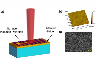 |
| This image shows a) Excitation by light of a surface plasmon-polariton on a thin film of titanium nitride. b) Atomic force microscope image of the surface of titanium nitride film. The mean roughness of the film is 0.5 nm. c) Scanning electron microscopy image of TiN thin film on sapphire. The texture shows multivariant epitaxial (crystalline) growth.
Credit: Alexandra Boltasseva, Purdue University/Optical Materials Express. |
Abstract:
Helping bridge the gap between photonics and electronics, researchers from Purdue University have coaxed a thin film of titanium nitride into transporting plasmons, tiny electron excitations coupled to light that can direct and manipulate optical signals on the nanoscale. Titanium nitride's addition to the short list of surface-plasmon-supporting materials, formerly comprised only of metals, could point the way to a new class of optoelectronic devices with unprecedented speed and efficiency.
Researchers discover a new path for light through metal: Novel plasmonic material may merge photonic and electronic technologies
Washington, DC | Posted on March 27th, 2012"We have found that titanium nitride is a promising candidate for an entirely new class of technologies based on plasmonics and metamaterials," said Alexandra Boltasseva, a researcher at Purdue and an author on a paper published today in the Optical Society's (OSA (http://www.osa.org)) open-access journal Optical Materials Express (http://www.opticsinfobase.org/ome). "This is particularly compelling because surface plasmons resolve a basic mismatch between wavelength-scale optical devices and the much smaller components of integrated electronic circuits."
Value of Plasmons
Metals carry electricity with ease, but normally do nothing to transmit light waves. Surface plasmons, unusual light-coupled oscillations that form on the surface of metallic materials, are the exception to that rule. When excited on the surface of metals by light waves of specific frequencies, plasmons are able to retain that same frequency, but with wavelengths that are orders-of-magnitude smaller, cramming visible and near-infrared light into the realm of the nanoscale.
In the world of electronics and optics, that 100-fold contraction is a boon. Circuits that direct the paths of electrons operate on a much smaller scale than optical light waves, so engineers must either rely on small but relatively sluggish electrons for information processing or bulk up to accommodate the zippy photons. Plasmons represent the best of both worlds and are already at the heart of a number of optoelectronic devices. They have not had widespread use, however, due to the dearth of materials that readily generate them and the fact that metals, in most cases, cannot be integrated with semiconductor devices.
Plasmonic Materials
Until now, the best candidates for plasmonic materials were gold and silver. These noble metals, however, are not compatible with standard silicon manufacturing technologies, limiting their use in commercial products. Silver is the metal with the best optical and surface plasmon properties, but it forms grainy, or semi-continuous, thin films. Silver also easily degrades in air, which causes loss of optical signal, making it a less-attractive material in plasmon technologies.
In an effort to overcome these drawbacks, Boltasseva and her team chose to study titanium nitride�a ceramic material that is commonly used as a barrier metal in microelectronics and to coat metal surfaces such as medical implants or machine tooling parts�because they could manipulate its properties in the manufacturing process. It also could be easily integrated into silicon products, and grown crystal-by-crystal, forming highly uniform, ultrathin films�properties that metals do not share.
To test its plasmonic capabilities, the researchers deposited a very thin, very even film of titanium nitride on a sapphire surface. They were able to confirm that titanium nitride supported the propagation of surface plasmons almost as efficiently as gold. Silver, under perfect conditions, was still more efficient for plasmonic applications, but its acknowledged signal loss limited its practical applications.
To further improve the performance of titanium nitride, the researchers are now looking into a manufacturing method known as molecular beam epitaxy, which would enable them to grow the films and layered structures known as superlattices crystal-by-crystal.
Technologies and Potential Applications
In addition to plasmonics, the researchers also speculate that titanium nitride may have applications in metamaterials, which are engineered materials that can be tailored for almost any application because of their extraordinary response to electromagnetic, acoustic, and thermal waves. Recently proposed applications of metamaterials include invisibility cloaks, optical black holes, nanoscale optics, data storage, and quantum information processing.
The search for alternatives to noble metals with improved optical properties, easier fabrication and integration capabilities could ultimately lead to real-life applications for plasmonics and metamaterials.
"Plasmonics is an important technology for nanoscale optical circuits, sensing, and data storage because it can focus light down to nanoscale," notes Boltasseva. "Titanium nitride is a promising candidate in the near-infrared and visible wavelength ranges. Unlike gold and silver, titanium nitride is compatible with standard semiconductor manufacturing technology and provides many advantages in its nanofabrication and integration."
According to the researchers, titanium nitride-based devices could provide nearly the same performance for some plasmonic applications. While noble metals like silver would still be the best choice for specific applications like negative index metamaterials, titanium nitride could outperform noble metals in other metamaterial and transformation optics devices, such as those based on hyperbolic metamaterials.
####
About Optical Society of America
Uniting more than 130,000 professionals from 175 countries, the Optical Society (OSA) brings together the global optics community through its programs and initiatives. Since 1916 OSA has worked to advance the common interests of the field, providing educational resources to the scientists, engineers and business leaders who work in the field by promoting the science of light and the advanced technologies made possible by optics and photonics. OSA publications, events, technical groups and programs foster optics knowledge and scientific collaboration among all those with an interest in optics and photonics. For more information, visit www.osa.org.
About Optical Materials Express
Optical Materials Express (OMEx) is OSA's newest peer-reviewed, open-access journal focusing on the synthesis, processing and characterization of materials for applications in optics and photonics. OMEx, which launched in April 2011, primarily emphasizes advances in novel optical materials, their properties, modeling, synthesis and fabrication techniques; how such materials contribute to novel optical behavior; and how they enable new or improved optical devices. For more information, visit www.OpticsInfoBase.org/OMEx.
For more information, please click here
Contacts:
Angela Stark
202-416-1443
Copyright © Optical Society of America
If you have a comment, please Contact us.Issuers of news releases, not 7th Wave, Inc. or Nanotechnology Now, are solely responsible for the accuracy of the content.
Bookmark:


| Related Links |
| Related News Press |
News and information
![]() Quantum computer improves AI predictions April 17th, 2026
Quantum computer improves AI predictions April 17th, 2026
![]() Flexible sensor gains sensitivity under pressure April 17th, 2026
Flexible sensor gains sensitivity under pressure April 17th, 2026
![]() A reusable chip for particulate matter sensing April 17th, 2026
A reusable chip for particulate matter sensing April 17th, 2026
![]() Detecting vibrational quantum beating in the predissociation dynamics of SF6 using time-resolved photoelectron spectroscopy April 17th, 2026
Detecting vibrational quantum beating in the predissociation dynamics of SF6 using time-resolved photoelectron spectroscopy April 17th, 2026
Thin films
![]() Tiny nanosheets, big leap: A new sensor detects ethanol at ultra-low levels January 30th, 2026
Tiny nanosheets, big leap: A new sensor detects ethanol at ultra-low levels January 30th, 2026
![]() Utilizing palladium for addressing contact issues of buried oxide thin film transistors April 5th, 2024
Utilizing palladium for addressing contact issues of buried oxide thin film transistors April 5th, 2024
![]() Understanding the mechanism of non-uniform formation of diamond film on tools: Paving the way to a dry process with less environmental impact March 24th, 2023
Understanding the mechanism of non-uniform formation of diamond film on tools: Paving the way to a dry process with less environmental impact March 24th, 2023
![]() New study introduces the best graphite films: The work by Distinguished Professor Feng Ding at UNIST has been published in the October 2022 issue of Nature Nanotechnology November 4th, 2022
New study introduces the best graphite films: The work by Distinguished Professor Feng Ding at UNIST has been published in the October 2022 issue of Nature Nanotechnology November 4th, 2022
Memory Technology
![]() Researchers tackle the memory bottleneck stalling quantum computing October 3rd, 2025
Researchers tackle the memory bottleneck stalling quantum computing October 3rd, 2025
![]() First real-time observation of two-dimensional melting process: Researchers at Mainz University unveil new insights into magnetic vortex structures August 8th, 2025
First real-time observation of two-dimensional melting process: Researchers at Mainz University unveil new insights into magnetic vortex structures August 8th, 2025
![]() Utilizing palladium for addressing contact issues of buried oxide thin film transistors April 5th, 2024
Utilizing palladium for addressing contact issues of buried oxide thin film transistors April 5th, 2024
Discoveries
![]() Quantum computer improves AI predictions April 17th, 2026
Quantum computer improves AI predictions April 17th, 2026
![]() Flexible sensor gains sensitivity under pressure April 17th, 2026
Flexible sensor gains sensitivity under pressure April 17th, 2026
![]() A reusable chip for particulate matter sensing April 17th, 2026
A reusable chip for particulate matter sensing April 17th, 2026
![]() Detecting vibrational quantum beating in the predissociation dynamics of SF6 using time-resolved photoelectron spectroscopy April 17th, 2026
Detecting vibrational quantum beating in the predissociation dynamics of SF6 using time-resolved photoelectron spectroscopy April 17th, 2026
Materials/Metamaterials/Magnetoresistance
![]() First real-time observation of two-dimensional melting process: Researchers at Mainz University unveil new insights into magnetic vortex structures August 8th, 2025
First real-time observation of two-dimensional melting process: Researchers at Mainz University unveil new insights into magnetic vortex structures August 8th, 2025
![]() Researchers unveil a groundbreaking clay-based solution to capture carbon dioxide and combat climate change June 6th, 2025
Researchers unveil a groundbreaking clay-based solution to capture carbon dioxide and combat climate change June 6th, 2025
![]() A 1960s idea inspires NBI researchers to study hitherto inaccessible quantum states June 6th, 2025
A 1960s idea inspires NBI researchers to study hitherto inaccessible quantum states June 6th, 2025
![]() Institute for Nanoscience hosts annual proposal planning meeting May 16th, 2025
Institute for Nanoscience hosts annual proposal planning meeting May 16th, 2025
Announcements
![]() A fundamentally new therapeutic approach to cystic fibrosis: Nanobody repairs cellular defect April 17th, 2026
A fundamentally new therapeutic approach to cystic fibrosis: Nanobody repairs cellular defect April 17th, 2026
![]() UC Irvine physicists discover method to reverse �quantum scrambling� : The work addresses the problem of information loss in quantum computing system April 17th, 2026
UC Irvine physicists discover method to reverse �quantum scrambling� : The work addresses the problem of information loss in quantum computing system April 17th, 2026
Photonics/Optics/Lasers
![]() Metasurfaces smooth light to boost magnetic sensing precision January 30th, 2026
Metasurfaces smooth light to boost magnetic sensing precision January 30th, 2026
![]() From sensors to smart systems: the rise of AI-driven photonic noses January 30th, 2026
From sensors to smart systems: the rise of AI-driven photonic noses January 30th, 2026
|
|
||
|
|
||
| The latest news from around the world, FREE | ||
|
|
||
|
|
||
| Premium Products | ||
|
|
||
|
Only the news you want to read!
Learn More |
||
|
|
||
|
Full-service, expert consulting
Learn More |
||
|
|
||