Home > Press > New photonic crystals have both electronic and optical properties
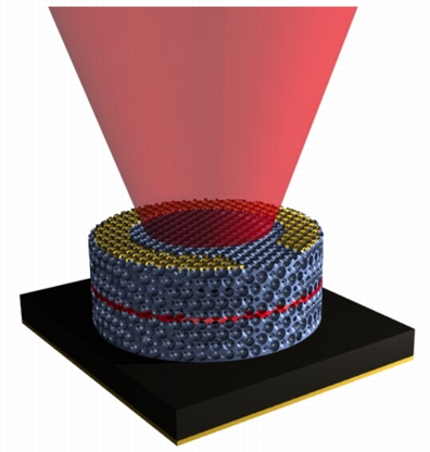 |
| Using an epitaxial approach, researchers developed a 3-D photonic crystal LED, the first such optoelectronic device. | Graphic by Eric Nelson |
Abstract:
In an advance that could open new avenues for solar cells, lasers, metamaterials and more, researchers at the University of Illinois have demonstrated the first optoelectronically active 3-D photonic crystal.
New photonic crystals have both electronic and optical properties
Champaign, IL | Posted on July 25th, 2011"We've discovered a way to change the three-dimensional structure of a well-established semiconductor material to enable new optical properties while maintaining its very attractive electrical properties," said Paul Braun, a professor of materials science and engineering and of chemistry who led the research effort.
The team published its advance in the journal Nature Materials.
Photonic crystals are materials that can control or manipulate light in unexpected ways thanks to their unique physical structures. Photonic crystals can induce unusual phenomena and affect photon behavior in ways that traditional optical materials and devices can't. They are popular materials of study for applications in lasers, solar energy, LEDs, metamaterials and more.
However, previous attempts at making 3-D photonic crystals have resulted in devices that are only optically active that is, they can direct light but not electronically active, so they can't turn electricity to light or vice versa.
The Illinois team's photonic crystal has both properties.
"With our approach to fabricating photonic crystals, there's a lot of potential to optimize electronic and optical properties simultaneously," said Erik Nelson, a former graduate student in Braun's lab who now is a postdoctoral researcher at Harvard University. "It gives you the opportunity to control light in ways that are very unique to control the way it's emitted and absorbed or how it propagates."
To create a 3-D photonic crystal that is both electronically and optically active, the researchers started with a template of tiny spheres packed together. Then, they deposit gallium arsenide (GaAs), a widely used semiconductor, through the template, filling in the gaps between the spheres.
The GaAs grows as a single crystal from the bottom up, a process called epitaxy. Epitaxy is common in industry to create flat, two-dimensional films of single-crystal semiconductors, but Braun's group developed a way to apply it to an intricate three-dimensional structure.
"The key discovery here was that we grew single-crystal semiconductor through this complex template," said Braun, who also is affiliated with the Beckman Institute for Advanced Science and Technology and with the Frederick Seitz Materials Research Laboratory at Illinois. "Gallium arsenide wants to grow as a film on the substrate from the bottom up, but it runs into the template and goes around it. It's almost as though the template is filling up with water. As long as you keep growing GaAs, it keeps filling the template from the bottom up until you reach the top surface."
The epitaxial approach eliminates many of the defects introduced by top-down fabrication methods, a popular pathway for creating 3-D photonic structures. Another advantage is the ease of creating layered heterostructures. For example, a quantum well layer could be introduced into the photonic crystal by partially filling the template with GaAs and then briefly switching the vapor stream to another material.
Once the template is full, the researchers remove the spheres, leaving a complex, porous 3-D structure of single-crystal semiconductor. Then they coat the entire structure with a very thin layer of a semiconductor with a wider bandgap to improve performance and prevent surface recombination.
To test their technique, the group built a 3-D photonic crystal LED the first such working device.
Now, Braun's group is working to optimize the structure for specific applications. The LED demonstrates that the concept produces functional devices, but by tweaking the structure or using other semiconductor materials, researchers can improve solar collection or target specific wavelengths for metamaterials applications or low-threshold lasers.
"From this point on, it's a matter of changing the device geometry to achieve whatever properties you want," Nelson said. It really opens up a whole new area of research into extremely efficient or novel energy devices.
The U.S. Department of Energy and the Army Research Office supported this work. Other Illinois faculty involved in the project are electrical and computer engineering professors James Coleman and Xiuling Li, and materials science and engineering professor John Rogers.
####
For more information, please click here
Contacts:
Liz Ahlberg
Physical Sciences Editor
217-244-1073
Paul Braun
217-244-7293
Copyright © University of Illinois at Urbana-Champaign
If you have a comment, please Contact us.Issuers of news releases, not 7th Wave, Inc. or Nanotechnology Now, are solely responsible for the accuracy of the content.
Bookmark:


| Related News Press |
News and information
![]() Decoding hydrogen‑bond network of electrolyte for cryogenic durable aqueous zinc‑ion batteries January 30th, 2026
Decoding hydrogen‑bond network of electrolyte for cryogenic durable aqueous zinc‑ion batteries January 30th, 2026
![]() COF scaffold membrane with gate‑lane nanostructure for efficient Li+/Mg2+ separation January 30th, 2026
COF scaffold membrane with gate‑lane nanostructure for efficient Li+/Mg2+ separation January 30th, 2026
Display technology/LEDs/SS Lighting/OLEDs
![]() Spinel-type sulfide semiconductors to operate the next-generation LEDs and solar cells For solar-cell absorbers and green-LED source October 3rd, 2025
Spinel-type sulfide semiconductors to operate the next-generation LEDs and solar cells For solar-cell absorbers and green-LED source October 3rd, 2025
![]() Efficient and stable hybrid perovskite-organic light-emitting diodes with external quantum efficiency exceeding 40 per cent July 5th, 2024
Efficient and stable hybrid perovskite-organic light-emitting diodes with external quantum efficiency exceeding 40 per cent July 5th, 2024
Discoveries
![]() From sensors to smart systems: the rise of AI-driven photonic noses January 30th, 2026
From sensors to smart systems: the rise of AI-driven photonic noses January 30th, 2026
![]() Decoding hydrogen‑bond network of electrolyte for cryogenic durable aqueous zinc‑ion batteries January 30th, 2026
Decoding hydrogen‑bond network of electrolyte for cryogenic durable aqueous zinc‑ion batteries January 30th, 2026
![]() COF scaffold membrane with gate‑lane nanostructure for efficient Li+/Mg2+ separation January 30th, 2026
COF scaffold membrane with gate‑lane nanostructure for efficient Li+/Mg2+ separation January 30th, 2026
Materials/Metamaterials/Magnetoresistance
![]() First real-time observation of two-dimensional melting process: Researchers at Mainz University unveil new insights into magnetic vortex structures August 8th, 2025
First real-time observation of two-dimensional melting process: Researchers at Mainz University unveil new insights into magnetic vortex structures August 8th, 2025
![]() Researchers unveil a groundbreaking clay-based solution to capture carbon dioxide and combat climate change June 6th, 2025
Researchers unveil a groundbreaking clay-based solution to capture carbon dioxide and combat climate change June 6th, 2025
![]() A 1960s idea inspires NBI researchers to study hitherto inaccessible quantum states June 6th, 2025
A 1960s idea inspires NBI researchers to study hitherto inaccessible quantum states June 6th, 2025
![]() Institute for Nanoscience hosts annual proposal planning meeting May 16th, 2025
Institute for Nanoscience hosts annual proposal planning meeting May 16th, 2025
Announcements
![]() Decoding hydrogen‑bond network of electrolyte for cryogenic durable aqueous zinc‑ion batteries January 30th, 2026
Decoding hydrogen‑bond network of electrolyte for cryogenic durable aqueous zinc‑ion batteries January 30th, 2026
![]() COF scaffold membrane with gate‑lane nanostructure for efficient Li+/Mg2+ separation January 30th, 2026
COF scaffold membrane with gate‑lane nanostructure for efficient Li+/Mg2+ separation January 30th, 2026
Energy
![]() Sensors innovations for smart lithium-based batteries: advancements, opportunities, and potential challenges August 8th, 2025
Sensors innovations for smart lithium-based batteries: advancements, opportunities, and potential challenges August 8th, 2025
![]() Simple algorithm paired with standard imaging tool could predict failure in lithium metal batteries August 8th, 2025
Simple algorithm paired with standard imaging tool could predict failure in lithium metal batteries August 8th, 2025
Photonics/Optics/Lasers
![]() Metasurfaces smooth light to boost magnetic sensing precision January 30th, 2026
Metasurfaces smooth light to boost magnetic sensing precision January 30th, 2026
![]() From sensors to smart systems: the rise of AI-driven photonic noses January 30th, 2026
From sensors to smart systems: the rise of AI-driven photonic noses January 30th, 2026
![]() ICFO researchers overcome long-standing bottleneck in single photon detection with twisted 2D materials August 8th, 2025
ICFO researchers overcome long-standing bottleneck in single photon detection with twisted 2D materials August 8th, 2025
Solar/Photovoltaic
![]() Spinel-type sulfide semiconductors to operate the next-generation LEDs and solar cells For solar-cell absorbers and green-LED source October 3rd, 2025
Spinel-type sulfide semiconductors to operate the next-generation LEDs and solar cells For solar-cell absorbers and green-LED source October 3rd, 2025
![]() KAIST researchers introduce new and improved, next-generation perovskite solar cell November 8th, 2024
KAIST researchers introduce new and improved, next-generation perovskite solar cell November 8th, 2024
![]() Groundbreaking precision in single-molecule optoelectronics August 16th, 2024
Groundbreaking precision in single-molecule optoelectronics August 16th, 2024
![]() Development of zinc oxide nanopagoda array photoelectrode: photoelectrochemical water-splitting hydrogen production January 12th, 2024
Development of zinc oxide nanopagoda array photoelectrode: photoelectrochemical water-splitting hydrogen production January 12th, 2024
|
|
||
|
|
||
| The latest news from around the world, FREE | ||
|
|
||
|
|
||
| Premium Products | ||
|
|
||
|
Only the news you want to read!
Learn More |
||
|
|
||
|
Full-service, expert consulting
Learn More |
||
|
|
||