Home > Press > Applied Materials’ New Enabler E5 System Solves Critical Contact Etch Challenges for 32nm Memory Chips
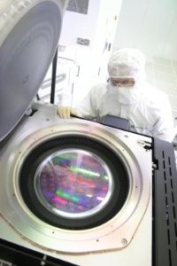 |
| The Applied Centura Enabler E5 sets an industry benchmark, enabling customers to etch 40:1 high aspect ratio contacts with the excellent profile control required for 32nm and below memory chip manufacturing. (Photo: Business Wire) |
Abstract:
Applied Materials, Inc. today unveiled its Applied Centura® Enabler® E5 dielectric etch system, the industry's most advanced solution for creating the 40:1 high aspect ratio contact features that are critical to the yield and performance of 32nm and below DRAM and Flash memory chips. The Enabler E5 sets a new benchmark in profile control, enabling customers to manufacture high performance, robust, next-generation memory devices with >80% bottom-to-top CD ratios across the wafer, and with less than 3nm bowing of the contact sidewall.
Applied Materials’ New Enabler E5 System Solves Critical Contact Etch Challenges for 32nm Memory Chips
SANTA CLARA, CA | Posted on December 3rd, 2008 "Next-generation Flash and DRAM devices pose a significant challenge for dielectric etch systems since it is very difficult to achieve the global profile control necessary for fabricating high aspect ratio contacts," said Ellie Yieh, vice president and general manager of Applied Materials' Etch and Cleans Business Unit. "The Enabler E5 is the only system that can meet all these requirements, allowing memory manufacturers to continue to increase density and reduce the cost-per-bit."
"Customers are very excited about the Enabler E5 system's exceptional profile control," added Ms. Yieh. "We're seeing strong demand for this product with multiple systems installed worldwide and repeat orders from leading memory manufacturers where it has solidly won multiple head-to-head run-offs with other systems."
Central to the Enabler E5 system's performance are its unique reactor architecture and precise process control that provide repeatable, uniform vertical profiles at high aspect ratios globally - from edge-to-edge and wafer-to-wafer - addressing a critical yield inhibitor at higher memory densities. The proprietary chamber technology also provides more efficient cleaning, delivering 50% longer between-maintenance intervals than any competitive system. For more information on the Applied Centura Enabler E5 system, please visit:
www.appliedmaterials.com/products/dielectric_etch_enabler_4.html.
####
About Applied Materials, Inc.
Applied Materials, Inc. (Nasdaq:AMAT) is the global leader in Nanomanufacturing Technology™ solutions with a broad portfolio of innovative equipment, service and software products for the fabrication of semiconductor chips, flat panel displays, solar photovoltaic cells, flexible electronics and energy efficient glass. At Applied Materials, we apply Nanomanufacturing Technology to improve the way people live.
For more information, please click here
Contacts:
Applied Materials, Inc.
Betty Newboe
408-563-0647 (editorial/media)
Robert Friess
408-986-7977 (financial community)
Copyright © Business Wire 2008
If you have a comment, please Contact us.Issuers of news releases, not 7th Wave, Inc. or Nanotechnology Now, are solely responsible for the accuracy of the content.
Bookmark:


| Related News Press |
News and information
![]() Quantum computer improves AI predictions April 17th, 2026
Quantum computer improves AI predictions April 17th, 2026
![]() Flexible sensor gains sensitivity under pressure April 17th, 2026
Flexible sensor gains sensitivity under pressure April 17th, 2026
![]() A reusable chip for particulate matter sensing April 17th, 2026
A reusable chip for particulate matter sensing April 17th, 2026
![]() Detecting vibrational quantum beating in the predissociation dynamics of SF6 using time-resolved photoelectron spectroscopy April 17th, 2026
Detecting vibrational quantum beating in the predissociation dynamics of SF6 using time-resolved photoelectron spectroscopy April 17th, 2026
Chip Technology
![]() A reusable chip for particulate matter sensing April 17th, 2026
A reusable chip for particulate matter sensing April 17th, 2026
![]() Metasurfaces smooth light to boost magnetic sensing precision January 30th, 2026
Metasurfaces smooth light to boost magnetic sensing precision January 30th, 2026
Announcements
![]() A fundamentally new therapeutic approach to cystic fibrosis: Nanobody repairs cellular defect April 17th, 2026
A fundamentally new therapeutic approach to cystic fibrosis: Nanobody repairs cellular defect April 17th, 2026
![]() UC Irvine physicists discover method to reverse ‘quantum scrambling’ : The work addresses the problem of information loss in quantum computing system April 17th, 2026
UC Irvine physicists discover method to reverse ‘quantum scrambling’ : The work addresses the problem of information loss in quantum computing system April 17th, 2026
Tools
![]() Metasurfaces smooth light to boost magnetic sensing precision January 30th, 2026
Metasurfaces smooth light to boost magnetic sensing precision January 30th, 2026
![]() From sensors to smart systems: the rise of AI-driven photonic noses January 30th, 2026
From sensors to smart systems: the rise of AI-driven photonic noses January 30th, 2026
![]() Japan launches fully domestically produced quantum computer: Expo visitors to experience quantum computing firsthand August 8th, 2025
Japan launches fully domestically produced quantum computer: Expo visitors to experience quantum computing firsthand August 8th, 2025
|
|
||
|
|
||
| The latest news from around the world, FREE | ||
|
|
||
|
|
||
| Premium Products | ||
|
|
||
|
Only the news you want to read!
Learn More |
||
|
|
||
|
Full-service, expert consulting
Learn More |
||
|
|
||