Home > Press > NIST ‘Stress Tests’ Probe Nanoscale Strains in Materials
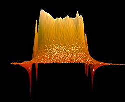 |
| Confocal Raman microscopy image of stress in a silicon crystal caused by indentation with a 20 micrometer long wedge. The image does not show the silicon but rather the magnitude of stress in the crystal, with compressive stress around the wedge going up from the base line. Vampiric red “fangs” reveal tensile stress associated with cracking at the ends of the indentation.
Credit: Stranick, NIST |
Abstract:
Researchers at the National Institute of Standards and Technology (NIST) have demonstrated their ability to measure relatively low levels of stress or strain in regions of a semiconductor device as small as 10 nanometers across. Their recent results* not only will impact the design of future generations of integrated circuits but also lay to rest a long-standing disagreement in results between two different methods for measuring stress in semiconductors.
NIST ‘Stress Tests’ Probe Nanoscale Strains in Materials
GAITHERSBURG, MD | Posted on November 25th, 2008Mechanical stress and strain in semiconductors and other devices is caused by atoms in the crystal lattice being compressed or stretched out of their preferred positions, a complex—and not always harmful—phenomenon. Stress in the underlying structure of light-emitting diodes and lasers can shift output colors and lower the device's lifetime. Stress in microelectromechanical systems can lead to fracture and buckling that also truncates their lifespan. On the other hand, stress is deliberately built into state-of-the-art microcircuits because properly applied it can increase the speed of transistors without making any other changes to the design. "Stress engineering has allowed the semiconductor industry to increase the performance of devices well beyond what was expected with the current materials set," said NIST research physicist Robert Cook, "thus avoiding the significant engineering problems and expense associated with changing materials."
Both the good and the bad stresses need to be measured, however, if they're to be controlled by device designers. As the component size of microcircuits has become smaller and smaller, this has become more difficult—particularly since two different and widely used methods of stress measurement have been returning disparate results. One, electron back scattered diffraction (EBSD), deduces underlying stress by observing the patterns of electrons scattered back from the crystal planes. The other, confocal Raman microscopy (CRM), measures minute shifts in the frequency of photons that interact with the atomic bonds in the crystal—shifts that change depending on the amount of stress on the bond. The NIST team used customized, highly sensitive versions of both instruments in a series of comparison measurements to resolve the discrepancies.
The key issue, they found, was depth of penetration of the two techniques. Electron beams sample only the top 20 or 30 nanometers of the material, Cook explained, while the laser-generated photons used in CRM might penetrate as deep as a micrometer or more. The NIST researchers found that by varying the wavelength of the Raman photons and positioning the focus of the microscope they could select the depth of the features measured by the Raman technique—and when the CRM was tuned for the topmost layers of the crystal, the results were in close agreement with EBSD measurements.
The NIST instruments also demonstrate the potential for using the two techniques in combination to make reliable, nanoscale measurements of stress in silicon, which enables device developers to optimize materials and processes. EBSD, although confined to near-surface stress, can make measurements with resolutions as small as 10 nanometers. CRM resolution is about 10 times coarser, but it can return depth profiles of stress.
* M.D. Vaudin, Y.B. Gerbig, S.J. Stranick and R.F. Cook. Comparison of nanoscale measurements of strain and stress using electron back scattered diffraction and confocal Raman microscopy. Applied Physics Letters 93, 193116. (2008)
####
About NIST
Founded in 1901, NIST is a non-regulatory federal agency within the U.S. Department of Commerce. NIST's mission is to promote U.S. innovation and industrial competitiveness by advancing measurement science, standards, and technology in ways that enhance economic security and improve our quality of life.
For more information, please click here
Contacts:
Michael Baum
(301) 975-2763
Copyright © NIST
If you have a comment, please Contact us.Issuers of news releases, not 7th Wave, Inc. or Nanotechnology Now, are solely responsible for the accuracy of the content.
Bookmark:


| Related News Press |
News and information
![]() Quantum computer improves AI predictions April 17th, 2026
Quantum computer improves AI predictions April 17th, 2026
![]() Flexible sensor gains sensitivity under pressure April 17th, 2026
Flexible sensor gains sensitivity under pressure April 17th, 2026
![]() A reusable chip for particulate matter sensing April 17th, 2026
A reusable chip for particulate matter sensing April 17th, 2026
![]() Detecting vibrational quantum beating in the predissociation dynamics of SF6 using time-resolved photoelectron spectroscopy April 17th, 2026
Detecting vibrational quantum beating in the predissociation dynamics of SF6 using time-resolved photoelectron spectroscopy April 17th, 2026
Govt.-Legislation/Regulation/Funding/Policy
![]() Quantum computer improves AI predictions April 17th, 2026
Quantum computer improves AI predictions April 17th, 2026
![]() Metasurfaces smooth light to boost magnetic sensing precision January 30th, 2026
Metasurfaces smooth light to boost magnetic sensing precision January 30th, 2026
![]() New imaging approach transforms study of bacterial biofilms August 8th, 2025
New imaging approach transforms study of bacterial biofilms August 8th, 2025
Discoveries
![]() Quantum computer improves AI predictions April 17th, 2026
Quantum computer improves AI predictions April 17th, 2026
![]() Flexible sensor gains sensitivity under pressure April 17th, 2026
Flexible sensor gains sensitivity under pressure April 17th, 2026
![]() A reusable chip for particulate matter sensing April 17th, 2026
A reusable chip for particulate matter sensing April 17th, 2026
![]() Detecting vibrational quantum beating in the predissociation dynamics of SF6 using time-resolved photoelectron spectroscopy April 17th, 2026
Detecting vibrational quantum beating in the predissociation dynamics of SF6 using time-resolved photoelectron spectroscopy April 17th, 2026
Announcements
![]() A fundamentally new therapeutic approach to cystic fibrosis: Nanobody repairs cellular defect April 17th, 2026
A fundamentally new therapeutic approach to cystic fibrosis: Nanobody repairs cellular defect April 17th, 2026
![]() UC Irvine physicists discover method to reverse ‘quantum scrambling’ : The work addresses the problem of information loss in quantum computing system April 17th, 2026
UC Irvine physicists discover method to reverse ‘quantum scrambling’ : The work addresses the problem of information loss in quantum computing system April 17th, 2026
|
|
||
|
|
||
| The latest news from around the world, FREE | ||
|
|
||
|
|
||
| Premium Products | ||
|
|
||
|
Only the news you want to read!
Learn More |
||
|
|
||
|
Full-service, expert consulting
Learn More |
||
|
|
||