Home > Press > Fujitsu Achieves Breakthrough with World's First New Carbon Nanotube Composite
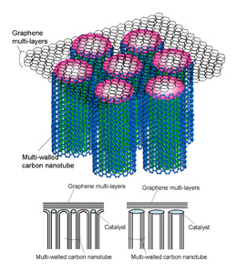 |
| Schematic view of the new nano-scale carbon composite (Lower image: Diagram of anticipated structure) |
Abstract:
- Features self-organizing carbon nanotubes and graphene -
Fujitsu Achieves Breakthrough with World's First New Carbon Nanotube Composite
Atsugi, Japan | Posted on March 2nd, 2008Fujitsu Laboratories Ltd. today announced the successful formation of a new nano-scale carbon composite featuring a self-organizing structure(1), by combining carbon nanotubes and graphene(2) which are both nano-scale carbon structures. The newly-discovered composite structure is synthesized at a temperature of 510 �C, cooler than for conventional graphene formed at temperatures too high for electronic device applications, thereby paving the way for the feasible use of graphene as a material suitable for future practical use in electronic devices which are vulnerable to heat. Carbon nanotubes have properties including high thermal conductivity and high current-density tolerance(3), while graphene is known for its high electron mobility. Carbon nanostructures combining these two materials hold the promise of creating new potential for material research and applications.
Details of this technology will be presented at the 34th Fullerene Nanotubes General Symposium to be held from March 3 to March 5 in Nagoya, Japan.
Background
Carbon nanotubes and graphene are both nano-scale structures consisting of carbon atoms. Graphene is a sheet-like hexagonal lattice of carbon atoms, while nanotubes can be described as graphene wrapped into a cylinder with a nano-scale diameter.
Despite the fact that both are made from the same carbon atoms, each has very distinct characteristics. Of any material found in nature, carbon nanotubes feature the highest thermal conductivity and mechanical strength as well as the ability to withstand the highest current density, making them an attractive material for wiring, heat dissipation, field electron emitters(4), and other potential applications. Research and development is underway to find technologies to synthesize carbon nanotubes at temperatures as low as approximately 400�C, a temperature that would enable its use in electronic devices vulnerable to heat. Since the discovery of its high electron mobility in 2004, graphene has become attractive as a channel material for future transistors. However, conventional methods for synthesizing graphene only work at temperatures over 700�C - considered too high for use in electronic devices - or involve a time-consuming and unreliable process of stripping away graphite crystals.
Fujitsu Laboratories is researching ways to develop electronic devices that take advantage of the superior properties of carbon nanostructures.
Overview of the New Technology
In order to better understand the growth mechanism of carbon nanotubes, Fujitsu Laboratories conducted experiments using chemical vapor deposition, a technique in which a feedstock gas is heat-cracked in a vacuum chamber to synthesize film or structures on a substrate. This resulted in the formation and discovery of aligned growth(5)multi-walled carbon nanotubes(6) featuring layers of graphene (from a few layers to a few dozen) on top formed in a self-organizing way, thereby forming a complex composite (see Figure 1).
Carbon-based materials come in a variety of different forms that depend on how their atoms link together, such as zero-dimensional fullerenes(7), one-dimensional nanotubes, two-dimensional (2-D) graphene, and three-dimensional (3-D) diamonds. Complex structures consisting of zero-dimensional and one-dimensional elements, known as "peapod(8)" structures, have already been created. The new complex composite developed by Fujitsu Laboratories is the world's first composite featuring one-dimensional and two-dimensional elements based on graphene layers and nanotubes, which are perpendicularly connected. The composite was synthesized at the relatively low temperature of 510�C.
Results
Due to the fact that carbon nanotubes are linear, one-dimensional structures, in the two-dimensional directions perpendicular to the tube axis they have nearly no thermal or electrical conductivity between tubes. Graphene, on the other hand, possesses electrical and thermal conductivity across two dimensions. The newly-discovered carbon nanostructure is expected to have electrical conduction and thermal dissipation in all directions. Conventionally aligned-growth carbon nanotubes have had relatively poor uniformity in length, thus being inconsistent when joined in the upper areas and resulting in increased thermal and electrical resistance. As the new carbon nanostructures from Fujitsu Labs feature carbon nanotubes that nearly all connect to the graphene with good uniformity at their endpoints (see Figure 2), and since the graphene surface is planar, it is anticipated that the new carbon nanostructures will enable excellent electrical and thermal conductivity. This technology brings the application of graphene for electronic devices one step closer to practical use.
Future Developments
Fujitsu Laboratories will continue to explore the mechanisms by which complex carbon nanostructures form and elucidate their physical characteristics, in order to develop electronic device application technologies that take advantage of those characteristics. In addition, in the field of material sciences Fujitsu Laboratories will pursue the development of technologies to enable the formation of high-quality carbon nanostructures at a lower temperature.
Glossary & Notes
1 Self-organizing structure:
Refers to a desired structure that self-forms naturally, without the need for complex controls.
2 Graphene:
A hexagonal lattice of carbon atoms. Graphite consists of layers of graphene stacked on top of each other.
3 Current-density tolerance:
The limit of high-density current that can flow through a material without changing its physical structure.
4 Field electron emitter:
A device that extracts electrons from a fixed surface employing an electrical field. Displays referred to as field-emission displays (FED) operate on the principle of electrons bumping up against fluorescent bodies, and causing them to emit light.
5 Aligned growth:
A growth pattern that grows perpendicular to a substrate.
6 Multi-walled carbon nanotube:
A type of carbon nanotube in which multiple graphene layers are arranged concentrically as a cylinder. Sizes vary in diameter from a few nanometers, to a few tens of nanometers.
7 Fullerene:
A molecule consisting of 60 carbon atoms arranged in a soccer-ball like structure.
8 Peapod:
A complex nanostructure consisting of fullerene laid out in a row inside a carbon nanotube. Named for its resemblance to a peapod.
####
About Fujitsu Laboratories Ltd.
Founded in 1968 as a wholly owned subsidiary of Fujitsu Limited, Fujitsu Laboratories Ltd. is one of the premier research centers in the world. With a global network of laboratories in Japan, China, the United States and Europe, the organization conducts a wide range of basic and applied research in the areas of Multimedia, Personal Systems, Networks, Peripherals, Advanced Materials and Electronic Devices.
For more information, please click here
Contacts:
Technical Contacts
Fujitsu Laboratories Ltd.
Nanotechnology R&D Center
Tel: +81-46-250-8234
Copyright © Fujitsu Laboratories Ltd.
If you have a comment, please Contact us.Issuers of news releases, not 7th Wave, Inc. or Nanotechnology Now, are solely responsible for the accuracy of the content.
Bookmark:


| Related News Press |
Events/Classes
![]() Institute for Nanoscience hosts annual proposal planning meeting May 16th, 2025
Institute for Nanoscience hosts annual proposal planning meeting May 16th, 2025
![]() A New Blue: Mysterious origin of the ribbontail ray�s electric blue spots revealed July 5th, 2024
A New Blue: Mysterious origin of the ribbontail ray�s electric blue spots revealed July 5th, 2024
![]() Researchers demonstrate co-propagation of quantum and classical signals: Study shows that quantum encryption can be implemented in existing fiber networks January 20th, 2023
Researchers demonstrate co-propagation of quantum and classical signals: Study shows that quantum encryption can be implemented in existing fiber networks January 20th, 2023
|
|
||
|
|
||
| The latest news from around the world, FREE | ||
|
|
||
|
|
||
| Premium Products | ||
|
|
||
|
Only the news you want to read!
Learn More |
||
|
|
||
|
Full-service, expert consulting
Learn More |
||
|
|
||