Home > Press > Carbon nanotube fabrication versatility is at the heart of innovative new materials growth tool
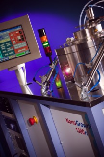 |
| Surrey NanoSystems is making its commercial debut at Nanotech 2007, offering what it believes is the most versatile growth tool for carbon nanotube fabrication ever produced. |
Abstract:
* tool provides practical platform for nanomaterial fabrication, from research to production
Carbon nanotube fabrication versatility is at the heart of innovative new materials growth tool
SANTA CLARA, CA | Posted on May 22nd, 2007Surrey NanoSystems is making its commercial debut at Nanotech 2007, offering what it believes is the most versatile growth tool for carbon nanotube fabrication ever produced, facilitating material growth at 'standard' temperatures in and around the 450-1000 degrees Celsius range, as well as growth at lower temperatures.
Called NanoGrowth 1000n, the new tool is purpose-designed for nanomaterial fabrication and comes with both CVD (chemical vapor deposition) and PECVD (plasma-enhanced CVD) processing capability. These two techniques provide great versatility for users.
Precision fabrication and configuration repeatability principles have been at the core of the tool's architecture, which has been developed by engineers with many years of experience of creating thin-film tools for both scientific research and commercial fabrication. Among the tool's many quality-oriented architectural features are an ultra-high purity gas delivery system and flexible closed-loop control systems that allow users to define target tolerances to achieve a high level of repeatability during all phases of the process.
A very high degree of hardware modularity allows the tool to be expanded easily and configured to meet current and future fabrication requirements. Among many options are further processing techniques such as ICP (inductively coupled plasma), dual sputter sources for catalyst deposition - including a module for delivery of vapor-phase catalysts like ferrocene - plus modules to add process stages for automated pilot production or high throughput. Included in the latter category are an automated wafer transport load/lock system, integrated etching capability, and a PECVD module for deposition of thin-film silicon-based materials.
"This new type of tool addresses the needs of nanomaterial researchers for stable and repeatable results, combined with the flexibility to accommodate individual development ideas. The tool's intrinsic hardware modularity allows users to gain automated control over all aspect of nanomaterial synthesis, from catalyst generation to final material processing," says Dr Guan Yow Chen, Chief Scientist at Surrey NanoSystems.
Users are provided with ready-to-use fabrication programs. These provide nanomaterial growth 'recipes' in the form of software templates that may be adapted easily by users for their own applications.
Surrey NanoSystems' new carbon nanotube tool is controlled by unique, touch-screen SCADA-style software (supervisory control and data acquisition) - developed and refined over more than seven years on high-end thin-film deposition tools. This software provides an extremely user-friendly interface that sits between the user and the tool - making complex growth or deposition processes both easy to create and run. MIMIC displays of the tool and other graphical techniques provide simple control over all phases of the material growth process, allowing the user to control every aspect - such as gas flow rate, temperatures, RF power, etc - manually or automatically.
Surrey NanoSystems expects the purpose-designed tool to enable nanomaterial researchers to shorten the path to commercialization. Nanomaterials are expected to have a huge impact on a wide range of next generation technologies such as sensors, interconnects, thermal heat sinks, displays, etc. One of the major goals behind the flexible architecture of the tool is making it possible to commercialize the use of carbon nanotubes and other nanowires in silicon chips - which are approaching their performance limits.
The recipes and patented fabrication technology inside the new tool are field proven, and derived from ground-breaking work by the University of Surrey's Advanced Technology Institute (ATI). IP Group PLC provided funding to create Surrey NanoSystems, a corporation dedicated to commercializing the process technology, which was established with staff and intellectual property from ATI and a leading thin-film deposition system manufacturer.
####
About Surrey NanoSystems
Surrey NanoSystems produces the world's most advanced tools and Carbon Nanotube processing recipes - making precision, repeatable nanotube and nanowire fabrication a reality. Our designed-for-purpose tools bridge the gap between R&D initiatives, and the volume production of commercial nanotechnology-based products.
For more information, please click here
Contacts:
Surrey NanoSystems
Euro Business Park, Building 24
Newhaven, BN9 0DQ, UK.
t: +44 (0)1273 515899;
Copyright © Surrey NanoSystems
If you have a comment, please Contact us.Issuers of news releases, not 7th Wave, Inc. or Nanotechnology Now, are solely responsible for the accuracy of the content.
Bookmark:


| Related News Press |
Nanotubes/Buckyballs/Fullerenes/Nanorods/Nanostrings/Nanosheets
![]() Tiny nanosheets, big leap: A new sensor detects ethanol at ultra-low levels January 30th, 2026
Tiny nanosheets, big leap: A new sensor detects ethanol at ultra-low levels January 30th, 2026
![]() Enhancing power factor of p- and n-type single-walled carbon nanotubes April 25th, 2025
Enhancing power factor of p- and n-type single-walled carbon nanotubes April 25th, 2025
![]() Chainmail-like material could be the future of armor: First 2D mechanically interlocked polymer exhibits exceptional flexibility and strength January 17th, 2025
Chainmail-like material could be the future of armor: First 2D mechanically interlocked polymer exhibits exceptional flexibility and strength January 17th, 2025
![]() Innovative biomimetic superhydrophobic coating combines repair and buffering properties for superior anti-erosion December 13th, 2024
Innovative biomimetic superhydrophobic coating combines repair and buffering properties for superior anti-erosion December 13th, 2024
Announcements
![]() A fundamentally new therapeutic approach to cystic fibrosis: Nanobody repairs cellular defect April 17th, 2026
A fundamentally new therapeutic approach to cystic fibrosis: Nanobody repairs cellular defect April 17th, 2026
![]() UC Irvine physicists discover method to reverse �quantum scrambling� : The work addresses the problem of information loss in quantum computing system April 17th, 2026
UC Irvine physicists discover method to reverse �quantum scrambling� : The work addresses the problem of information loss in quantum computing system April 17th, 2026
Tools
![]() Metasurfaces smooth light to boost magnetic sensing precision January 30th, 2026
Metasurfaces smooth light to boost magnetic sensing precision January 30th, 2026
![]() From sensors to smart systems: the rise of AI-driven photonic noses January 30th, 2026
From sensors to smart systems: the rise of AI-driven photonic noses January 30th, 2026
![]() Japan launches fully domestically produced quantum computer: Expo visitors to experience quantum computing firsthand August 8th, 2025
Japan launches fully domestically produced quantum computer: Expo visitors to experience quantum computing firsthand August 8th, 2025
|
|
||
|
|
||
| The latest news from around the world, FREE | ||
|
|
||
|
|
||
| Premium Products | ||
|
|
||
|
Only the news you want to read!
Learn More |
||
|
|
||
|
Full-service, expert consulting
Learn More |
||
|
|
||