Home > Press > Thinking thin brings new layering and thermal abilities to the semiconductor industry: In a breakthrough for the semiconductor industry, researchers demonstrate a new layer transfer technique called "controlled spalling" that creates many thin layers from a single gallium nitride
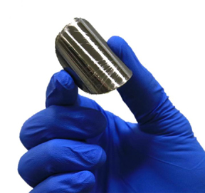 |
| The same 20-micron spalled GaN film, demonstrating the film's flexibility. CREDIT Bedell/IBM Research |
Abstract:
What would a simple technique to remove thin layers from otherwise thick, rigid semiconductor crystals mean for the semiconductor industry? This concept has been actively explored for years, as integrated circuits made on thin layers hold promise for developments including improved thermal characteristics, lightweight stackability and a high degree of flexibility compared to conventionally thick substrates.
Thinking thin brings new layering and thermal abilities to the semiconductor industry: In a breakthrough for the semiconductor industry, researchers demonstrate a new layer transfer technique called "controlled spalling" that creates many thin layers from a single gallium nitride
Washington, DC | Posted on July 11th, 2017In a significant advance, a research group from IBM successfully applied their new "controlled spalling" layer transfer technique to gallium nitride (GaN) crystals, a prevalent semiconductor material, and created a pathway for producing many layers from a single substrate.
As they report in the Journal of Applied Physics, from AIP Publishing, controlled spalling can be used to produce thin layers from thick GaN crystals without causing crystalline damage. The technique also makes it possible to measure basic physical properties of the material system, like strain-induced optical effects and fracture toughness, which are otherwise difficult to measure.
Single-crystal GaN wafers are extremely expensive, where just one 2-inch wafer can cost thousands of dollars, so having more layers means getting more value out of each wafer. Thinner layers also provide performance advantages for power electronics, since it offers lower electrical resistance and heat is easier to remove.
"Our approach to thin film removal is intriguing because it's based on fracture," said Stephen W. Bedell, research staff member at IBM Research and one of the paper's authors. "First, we first deposit a nickel layer onto the surface of the material we want to remove. This nickel layer is under tensile strength -- think drumhead. Then we simply roll a layer of tape onto the nickel, hold the substrate down so it can't move, and then peel the tape off. When we do this, the stressed nickel layer creates a crack in the underlying material that goes down into the substrate and then travels parallel to the surface."
Their method boils down to simply peeling off the tape, nickel layer and a thin layer of the substrate material stuck to the nickel.
"A good analogy of how remarkable this process is can be made with a pane of glass," Bedell said. "We're breaking the glass in the long direction, so instead of a bunch of broken glass shards, we're left with two full sheets of glass. We can control how much of the surface is removed by adjusting the thickness of the nickel layer. Because the entire process is done at room temperature, we can even do this on finished circuits and devices, rendering them flexible."
The group's work is noteworthy for multiple reasons. For starters, it's by far the simplest method of transferring thin layers from thick substrates. And it may well be the only layer transfer method that's materially agnostic.
"We've already demonstrated the transfer of silicon, germanium, gallium arsenide, gallium nitride/sapphire, and even amorphous materials like glass, and it can be applied at nearly any time in the fabrication flow, from starting materials to partially or fully finished circuits," Bedell said.
Turning a parlor trick into a reliable process, working to ensure that this approach would be a consistent technique for crack-free transfer, led to surprises along the way.
"The basic mechanism of substrate spalling fracture started out as a materials science problem," he said. "It was known that metallic film deposition would often lead to cracking of the underlying substrate, which is considered a bad thing. But we found that this was a metastable phenomenon, meaning that we could deposit a thick enough layer to crack the substrate, but thin enough so that it didn't crack on its own -- it just needed a crack to get started."
Their next discovery was how to make the crack initiation consistent and reliable. While there are many ways to generate a crack -- laser, chemical etching, thermal, mechanical, etc. -- it turns out that the simplest way, according to Bedell, is to terminate the thickness of the nickel layer very abruptly near the edge of the substrate.
"This creates a large stress discontinuity at the edge of the nickel film so that once the tape is applied, a small pull on the tape consistently initiates the crack in that region," he said.
Though it may not be obvious, gallium nitride is a vital material to our everyday lives. It's the underlying material used to fabricate blue, and now white, LEDs (for which the 2014 Nobel Prize in physics was awarded) as well as for high-power, high-voltage electronics. It may also prove useful for inherent biocompatibility, which when combined with control spalling may permit ultrathin bioelectronics or implantable sensors.
"Controlled spalling has already been used to create extremely lightweight, high-efficiency GaAs-based solar cells for aerospace applications and flexible state-of-the-art circuits," Bedell said.
The group is now working with research partners to fabricate high-voltage GaN devices using this approach. "We've also had great interaction with many of the GaN technology leaders through the Department of Energy's ARPA-E SWITCHES program and hope to use controlled spalling to enable novel devices through future partnerships," Bedell said.
####
About American Institute of Physics
The Journal of Applied Physics is an influential international journal publishing significant new experimental and theoretical results of applied physics research. See http://jap.aip.org .
For more information, please click here
Contacts:
Julia Majors
301-209-3090
Copyright © American Institute of Physics
If you have a comment, please Contact us.Issuers of news releases, not 7th Wave, Inc. or Nanotechnology Now, are solely responsible for the accuracy of the content.
Bookmark:


| Related Links |
| Related News Press |
News and information
![]() Simulating magnetization in a Heisenberg quantum spin chain April 5th, 2024
Simulating magnetization in a Heisenberg quantum spin chain April 5th, 2024
![]() NRL charters Navy�s quantum inertial navigation path to reduce drift April 5th, 2024
NRL charters Navy�s quantum inertial navigation path to reduce drift April 5th, 2024
![]() Discovery points path to flash-like memory for storing qubits: Rice find could hasten development of nonvolatile quantum memory April 5th, 2024
Discovery points path to flash-like memory for storing qubits: Rice find could hasten development of nonvolatile quantum memory April 5th, 2024
![]() Good as gold - improving infectious disease testing with gold nanoparticles April 5th, 2024
Good as gold - improving infectious disease testing with gold nanoparticles April 5th, 2024
Thin films
![]() Utilizing palladium for addressing contact issues of buried oxide thin film transistors April 5th, 2024
Utilizing palladium for addressing contact issues of buried oxide thin film transistors April 5th, 2024
![]() Understanding the mechanism of non-uniform formation of diamond film on tools: Paving the way to a dry process with less environmental impact March 24th, 2023
Understanding the mechanism of non-uniform formation of diamond film on tools: Paving the way to a dry process with less environmental impact March 24th, 2023
![]() New study introduces the best graphite films: The work by Distinguished Professor Feng Ding at UNIST has been published in the October 2022 issue of Nature Nanotechnology November 4th, 2022
New study introduces the best graphite films: The work by Distinguished Professor Feng Ding at UNIST has been published in the October 2022 issue of Nature Nanotechnology November 4th, 2022
![]() Thin-film, high-frequency antenna array offers new flexibility for wireless communications November 5th, 2021
Thin-film, high-frequency antenna array offers new flexibility for wireless communications November 5th, 2021
Hardware
![]() The present and future of computing get a boost from new research July 21st, 2023
The present and future of computing get a boost from new research July 21st, 2023
Possible Futures
![]() Discovery points path to flash-like memory for storing qubits: Rice find could hasten development of nonvolatile quantum memory April 5th, 2024
Discovery points path to flash-like memory for storing qubits: Rice find could hasten development of nonvolatile quantum memory April 5th, 2024
![]() With VECSELs towards the quantum internet Fraunhofer: IAF achieves record output power with VECSEL for quantum frequency converters April 5th, 2024
With VECSELs towards the quantum internet Fraunhofer: IAF achieves record output power with VECSEL for quantum frequency converters April 5th, 2024
Chip Technology
![]() Discovery points path to flash-like memory for storing qubits: Rice find could hasten development of nonvolatile quantum memory April 5th, 2024
Discovery points path to flash-like memory for storing qubits: Rice find could hasten development of nonvolatile quantum memory April 5th, 2024
![]() Utilizing palladium for addressing contact issues of buried oxide thin film transistors April 5th, 2024
Utilizing palladium for addressing contact issues of buried oxide thin film transistors April 5th, 2024
![]() HKUST researchers develop new integration technique for efficient coupling of III-V and silicon February 16th, 2024
HKUST researchers develop new integration technique for efficient coupling of III-V and silicon February 16th, 2024
Nanoelectronics
![]() Interdisciplinary: Rice team tackles the future of semiconductors Multiferroics could be the key to ultralow-energy computing October 6th, 2023
Interdisciplinary: Rice team tackles the future of semiconductors Multiferroics could be the key to ultralow-energy computing October 6th, 2023
![]() Key element for a scalable quantum computer: Physicists from Forschungszentrum J�lich and RWTH Aachen University demonstrate electron transport on a quantum chip September 23rd, 2022
Key element for a scalable quantum computer: Physicists from Forschungszentrum J�lich and RWTH Aachen University demonstrate electron transport on a quantum chip September 23rd, 2022
![]() Reduced power consumption in semiconductor devices September 23rd, 2022
Reduced power consumption in semiconductor devices September 23rd, 2022
![]() Atomic level deposition to extend Moore�s law and beyond July 15th, 2022
Atomic level deposition to extend Moore�s law and beyond July 15th, 2022
Discoveries
![]() Chemical reactions can scramble quantum information as well as black holes April 5th, 2024
Chemical reactions can scramble quantum information as well as black holes April 5th, 2024
![]() New micromaterial releases nanoparticles that selectively destroy cancer cells April 5th, 2024
New micromaterial releases nanoparticles that selectively destroy cancer cells April 5th, 2024
![]() Utilizing palladium for addressing contact issues of buried oxide thin film transistors April 5th, 2024
Utilizing palladium for addressing contact issues of buried oxide thin film transistors April 5th, 2024
Announcements
![]() NRL charters Navy�s quantum inertial navigation path to reduce drift April 5th, 2024
NRL charters Navy�s quantum inertial navigation path to reduce drift April 5th, 2024
![]() Discovery points path to flash-like memory for storing qubits: Rice find could hasten development of nonvolatile quantum memory April 5th, 2024
Discovery points path to flash-like memory for storing qubits: Rice find could hasten development of nonvolatile quantum memory April 5th, 2024
Interviews/Book Reviews/Essays/Reports/Podcasts/Journals/White papers/Posters
![]() Simulating magnetization in a Heisenberg quantum spin chain April 5th, 2024
Simulating magnetization in a Heisenberg quantum spin chain April 5th, 2024
![]() Discovery points path to flash-like memory for storing qubits: Rice find could hasten development of nonvolatile quantum memory April 5th, 2024
Discovery points path to flash-like memory for storing qubits: Rice find could hasten development of nonvolatile quantum memory April 5th, 2024
Aerospace/Space
![]() Under pressure - space exploration in our time: Advancing space exploration through diverse collaborations and ethical policies February 16th, 2024
Under pressure - space exploration in our time: Advancing space exploration through diverse collaborations and ethical policies February 16th, 2024
![]() Bridging light and electrons January 12th, 2024
Bridging light and electrons January 12th, 2024
![]() Manufacturing advances bring material back in vogue January 20th, 2023
Manufacturing advances bring material back in vogue January 20th, 2023
Solar/Photovoltaic
![]() Development of zinc oxide nanopagoda array photoelectrode: photoelectrochemical water-splitting hydrogen production January 12th, 2024
Development of zinc oxide nanopagoda array photoelectrode: photoelectrochemical water-splitting hydrogen production January 12th, 2024
![]() Shedding light on unique conduction mechanisms in a new type of perovskite oxide November 17th, 2023
Shedding light on unique conduction mechanisms in a new type of perovskite oxide November 17th, 2023
![]() Inverted perovskite solar cell breaks 25% efficiency record: Researchers improve cell efficiency using a combination of molecules to address different November 17th, 2023
Inverted perovskite solar cell breaks 25% efficiency record: Researchers improve cell efficiency using a combination of molecules to address different November 17th, 2023
![]() Charged �molecular beasts� the basis for new compounds: Researchers at Leipzig University use �aggressive� fragments of molecular ions for chemical synthesis November 3rd, 2023
Charged �molecular beasts� the basis for new compounds: Researchers at Leipzig University use �aggressive� fragments of molecular ions for chemical synthesis November 3rd, 2023
|
|
||
|
|
||
| The latest news from around the world, FREE | ||
|
|
||
|
|
||
| Premium Products | ||
|
|
||
|
Only the news you want to read!
Learn More |
||
|
|
||
|
Full-service, expert consulting
Learn More |
||
|
|
||