Home > Press > Researchers “iron out” graphene’s wrinkles: New technique produces highly conductive graphene wafers
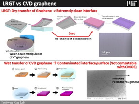 |
| MIT engineers have produced wrinkle-free graphene through a layer-resolved graphene transfer (LRGT) process, using an adhesive-like layer of nickel to peel graphene from silicon carbide. By then placing the graphene on an oxidized wafer of silicon, the nanometer-scale wrinkles are instantly flattened. Conventional chemical vapor deposition (CVD), in contrast, produces micron-scale wrinkles, with poor electrical performance. Courtesy of the researchers |
Abstract:
From an electron’s point of view, graphene must be a hair-raising thrill ride. For years, scientists have observed that electrons can blitz through graphene at velocities approaching the speed of light, far faster than they can travel through silicon and other semiconducting materials.
Researchers “iron out” graphene’s wrinkles: New technique produces highly conductive graphene wafers
Cambridge, MA | Posted on April 3rd, 2017Graphene, therefore, has been touted as a promising successor to silicon, with the potential to enable faster, more efficient electronic and photonic devices.
But manufacturing pristine graphene — a single, perfectly flat, ultrathin sheet of carbon atoms, precisely aligned and linked together like chickenwire — is extremely difficult. Conventional fabrication processes often generate wrinkles, which can derail an electron’s bullet-train journey, significantly limiting graphene’s electrical performance.
Now engineers at MIT have found a way to make graphene with fewer wrinkles, and to iron out the wrinkles that do appear. After fabricating and then flattening out the graphene, the researchers tested its electrical conductivity. They found each wafer exhibited uniform performance, meaning that electrons flowed freely across each wafer, at similar speeds, even across previously wrinkled regions.
In a paper published today in the Proceedings of the National Academy of Sciences, the researchers report that their techniques successfully produce wafer-scale, “single-domain” graphene — single layers of graphene that are uniform in both atomic arrangement and electronic performance.
“For graphene to play as a main semiconductor material for industry, it has to be single-domain, so that if you make millions of devices on it, the performance of the devices is the same in any location,” says Jeehwan Kim, the Class of 1947 Career Development Assistant Professor in the departments of Mechanical Engineering and Materials Science and Engineering at MIT. “Now we can really produce single-domain graphene at wafer scale.”
Kim’s co-authors include Sanghoon Bae, Samuel Cruz, and Yunjo Kim from MIT, along with researchers from IBM, the University of California at Los Angeles, and Kyungpook National University in South Korea.
A patchwork of wrinkles
The most common way to make graphene involves chemical vapor deposition, or CVD, a process in which carbon atoms are deposited onto a crystalline substrate such as copper foil. Once the copper foil is evenly coated with a single layer of carbon atoms, scientists submerge the entire thing in acid to etch away the copper. What remains is a single sheet of graphene, which researchers then pull out from the acid.
The CVD process can produce relatively large, macroscropic wrinkles in graphene, due to the roughness of the underlying copper itself and the process of pulling the graphene out from the acid. The alignment of carbon atoms is not uniform across the graphene, creating a “polycrystalline” state in which graphene resembles an uneven, patchwork terrain, preventing electrons from flowing at uniform rates.
In 2013, while working at IBM, Kim and his colleagues developed a method to fabricate wafers of single-crystalline graphene, in which the orientation of carbon atoms is exactly the same throughout a wafer.
Rather than using CVD, his team produced single-crystalline graphene from a silicon carbide wafer with an atomically smooth surface, albeit with tiny, step-like wrinkles on the order of several nanometers. They then used a thin sheet of nickel to peel off the topmost graphene from the silicon carbide wafer, in a process called layer-resolved graphene transfer.
Ironing charges
In their new paper, Kim and his colleagues discovered that the layer-resolved graphene transfer irons out the steps and tiny wrinkles in silicon carbide-fabricated graphene. Before transferring the layer of graphene onto a silicon wafer, the team oxidized the silicon, creating a layer of silicon dioxide that naturally exhibits electrostatic charges. When the researchers then deposited the graphene, the silicon dioxide effectively pulled graphene’s carbon atoms down onto the wafer, flattening out its steps and wrinkles.
Kim says this ironing method would not work on CVD-fabricated graphene, as the wrinkles generated through CVD are much larger, on the order of several microns.
“The CVD process creates wrinkles that are too high to be ironed out,” Kim notes. “For silicon carbide graphene, the wrinkles are just a few nanometers high, short enough to be flattened out.”
To test whether the flattened, single-crystalline graphene wafers were single-domain, the researchers fabricated tiny transistors on multiple sites on each wafer, including across previously wrinkled regions.
“We measured electron mobility throughout the wafers, and their performance was comparable,” Kim says. “What’s more, this mobility in ironed graphene is two times faster. So now we really have single-domain graphene, and its electrical quality is much higher [than graphene-attached silicon carbide].”
Kim says that while there are still challenges to adapting graphene for use in electronics, the group’s results give researchers a blueprint for how to reliably manufacture pristine, single-domain, wrinkle-free graphene at wafer scale.
“If you want to make any electronic device using graphene, you need to work with single-domain graphene,” Kim says. “There’s still a long way to go to make an operational transistor out of graphene. But we can now show the community guidelines for how you can make single-crystalline, single-domain graphene.”
###
Written by Jennifer Chu, MIT News Office
####
For more information, please click here
Contacts:
Abby Abazorius
MIT News Office
617.253.2709
Copyright © Massachusetts Institute of Technology
If you have a comment, please Contact us.Issuers of news releases, not 7th Wave, Inc. or Nanotechnology Now, are solely responsible for the accuracy of the content.
Bookmark:


| Related Links |
| Related News Press |
News and information
![]() Simulating magnetization in a Heisenberg quantum spin chain April 5th, 2024
Simulating magnetization in a Heisenberg quantum spin chain April 5th, 2024
![]() NRL charters Navy’s quantum inertial navigation path to reduce drift April 5th, 2024
NRL charters Navy’s quantum inertial navigation path to reduce drift April 5th, 2024
![]() Discovery points path to flash-like memory for storing qubits: Rice find could hasten development of nonvolatile quantum memory April 5th, 2024
Discovery points path to flash-like memory for storing qubits: Rice find could hasten development of nonvolatile quantum memory April 5th, 2024
2 Dimensional Materials
![]() NRL discovers two-dimensional waveguides February 16th, 2024
NRL discovers two-dimensional waveguides February 16th, 2024
Graphene/ Graphite
![]() NRL discovers two-dimensional waveguides February 16th, 2024
NRL discovers two-dimensional waveguides February 16th, 2024
Possible Futures
![]() Discovery points path to flash-like memory for storing qubits: Rice find could hasten development of nonvolatile quantum memory April 5th, 2024
Discovery points path to flash-like memory for storing qubits: Rice find could hasten development of nonvolatile quantum memory April 5th, 2024
![]() With VECSELs towards the quantum internet Fraunhofer: IAF achieves record output power with VECSEL for quantum frequency converters April 5th, 2024
With VECSELs towards the quantum internet Fraunhofer: IAF achieves record output power with VECSEL for quantum frequency converters April 5th, 2024
Chip Technology
![]() Discovery points path to flash-like memory for storing qubits: Rice find could hasten development of nonvolatile quantum memory April 5th, 2024
Discovery points path to flash-like memory for storing qubits: Rice find could hasten development of nonvolatile quantum memory April 5th, 2024
![]() Utilizing palladium for addressing contact issues of buried oxide thin film transistors April 5th, 2024
Utilizing palladium for addressing contact issues of buried oxide thin film transistors April 5th, 2024
![]() HKUST researchers develop new integration technique for efficient coupling of III-V and silicon February 16th, 2024
HKUST researchers develop new integration technique for efficient coupling of III-V and silicon February 16th, 2024
Optical computing/Photonic computing
![]() With VECSELs towards the quantum internet Fraunhofer: IAF achieves record output power with VECSEL for quantum frequency converters April 5th, 2024
With VECSELs towards the quantum internet Fraunhofer: IAF achieves record output power with VECSEL for quantum frequency converters April 5th, 2024
![]() Chemical reactions can scramble quantum information as well as black holes April 5th, 2024
Chemical reactions can scramble quantum information as well as black holes April 5th, 2024
![]() Optically trapped quantum droplets of light can bind together to form macroscopic complexes March 8th, 2024
Optically trapped quantum droplets of light can bind together to form macroscopic complexes March 8th, 2024
![]() HKUST researchers develop new integration technique for efficient coupling of III-V and silicon February 16th, 2024
HKUST researchers develop new integration technique for efficient coupling of III-V and silicon February 16th, 2024
Nanoelectronics
![]() Interdisciplinary: Rice team tackles the future of semiconductors Multiferroics could be the key to ultralow-energy computing October 6th, 2023
Interdisciplinary: Rice team tackles the future of semiconductors Multiferroics could be the key to ultralow-energy computing October 6th, 2023
![]() Key element for a scalable quantum computer: Physicists from Forschungszentrum Jülich and RWTH Aachen University demonstrate electron transport on a quantum chip September 23rd, 2022
Key element for a scalable quantum computer: Physicists from Forschungszentrum Jülich and RWTH Aachen University demonstrate electron transport on a quantum chip September 23rd, 2022
![]() Reduced power consumption in semiconductor devices September 23rd, 2022
Reduced power consumption in semiconductor devices September 23rd, 2022
![]() Atomic level deposition to extend Moore’s law and beyond July 15th, 2022
Atomic level deposition to extend Moore’s law and beyond July 15th, 2022
Discoveries
![]() Chemical reactions can scramble quantum information as well as black holes April 5th, 2024
Chemical reactions can scramble quantum information as well as black holes April 5th, 2024
![]() New micromaterial releases nanoparticles that selectively destroy cancer cells April 5th, 2024
New micromaterial releases nanoparticles that selectively destroy cancer cells April 5th, 2024
![]() Utilizing palladium for addressing contact issues of buried oxide thin film transistors April 5th, 2024
Utilizing palladium for addressing contact issues of buried oxide thin film transistors April 5th, 2024
Materials/Metamaterials/Magnetoresistance
![]() Nanoscale CL thermometry with lanthanide-doped heavy-metal oxide in TEM March 8th, 2024
Nanoscale CL thermometry with lanthanide-doped heavy-metal oxide in TEM March 8th, 2024
![]() Focused ion beam technology: A single tool for a wide range of applications January 12th, 2024
Focused ion beam technology: A single tool for a wide range of applications January 12th, 2024
Announcements
![]() NRL charters Navy’s quantum inertial navigation path to reduce drift April 5th, 2024
NRL charters Navy’s quantum inertial navigation path to reduce drift April 5th, 2024
![]() Discovery points path to flash-like memory for storing qubits: Rice find could hasten development of nonvolatile quantum memory April 5th, 2024
Discovery points path to flash-like memory for storing qubits: Rice find could hasten development of nonvolatile quantum memory April 5th, 2024
Interviews/Book Reviews/Essays/Reports/Podcasts/Journals/White papers/Posters
![]() Simulating magnetization in a Heisenberg quantum spin chain April 5th, 2024
Simulating magnetization in a Heisenberg quantum spin chain April 5th, 2024
![]() Discovery points path to flash-like memory for storing qubits: Rice find could hasten development of nonvolatile quantum memory April 5th, 2024
Discovery points path to flash-like memory for storing qubits: Rice find could hasten development of nonvolatile quantum memory April 5th, 2024
Photonics/Optics/Lasers
![]() With VECSELs towards the quantum internet Fraunhofer: IAF achieves record output power with VECSEL for quantum frequency converters April 5th, 2024
With VECSELs towards the quantum internet Fraunhofer: IAF achieves record output power with VECSEL for quantum frequency converters April 5th, 2024
![]() Nanoscale CL thermometry with lanthanide-doped heavy-metal oxide in TEM March 8th, 2024
Nanoscale CL thermometry with lanthanide-doped heavy-metal oxide in TEM March 8th, 2024
![]() Optically trapped quantum droplets of light can bind together to form macroscopic complexes March 8th, 2024
Optically trapped quantum droplets of light can bind together to form macroscopic complexes March 8th, 2024
![]() HKUST researchers develop new integration technique for efficient coupling of III-V and silicon February 16th, 2024
HKUST researchers develop new integration technique for efficient coupling of III-V and silicon February 16th, 2024
|
|
||
|
|
||
| The latest news from around the world, FREE | ||
|
|
||
|
|
||
| Premium Products | ||
|
|
||
|
Only the news you want to read!
Learn More |
||
|
|
||
|
Full-service, expert consulting
Learn More |
||
|
|
||