Home > Press > FEI Releases New Electronics Failure Analysis Applications for Helios NanoLab DualBeam Portfolio: Dx gas chemistry enables rapid delayering of ICs, while AutoLX advanced automation simplifies sample preparation for transmission electron microscopy
 |
Abstract:
FEI (NASDAQ: FEIC) announced today the release of two new application packages for its third-generation Helios NanoLab™ DualBeam™ systems, including the latest addition to the family, the plasma-sourced Helios PFIB. The new application solutions address needs in integrated device (IC) manufacturing and failure analysis for fast plan-view delayering, and rapid, automated preparation of ultrathin samples for imaging and analysis in a transmission electron microscope (TEM). The application packages are designed to work with various configurations of the Helios platform, including liquid metal (Ga) and plasma (Xe) ion sources.
FEI Releases New Electronics Failure Analysis Applications for Helios NanoLab DualBeam Portfolio: Dx gas chemistry enables rapid delayering of ICs, while AutoLX advanced automation simplifies sample preparation for transmission electron microscopy
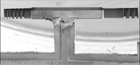
Hillsboro, OR | Posted on November 3rd, 2014"Delayering of IC devices is an important tool for semiconductor failure analysis, reverse engineering and circuit edit activities," said Rob Krueger, vice president and general manager of Electronics for FEI. "The new Dx beam chemistry delivers excellent planarity during delayering of mixed field regions, especially for technology nodes of 28nm and below where traditional methods are no longer viable. We have seen high-quality results using both Ga and Xe focused ion beams (FIBs) for front-side and back-side delayering. An additional benefit of switching to Dx for delayering is that the sidewalls of the milled trench are no longer conductive, so we can maintain device functionality if needed."
Paul Kirby, FEI's senior product marketing manager for Electronics, added, "TEM analysis is becoming nearly indispensable for process control and failure analysis at advanced nodes where device features are too small to be seen by more conventional SEM-based methods. Automated preparation of ultrathin samples that are only a few tens of nanometers thick, which is required for TEM, has contributed to greatly increased productivity and reliability of TEM analysis. The new AutoLXTM package, based on FEI's iFast Automation software, fully automates the in-situ lift out process, which locates and extracts a site-specific thick section containing the targeted feature and mounts it on a grid ready to be thinned to its final dimensions. For labs already using iFast recipes to create these thick samples, the addition of the AutoLX package opens up the door to increased productivity and more efficient use of valuable human resources."
The DualBeam's ability to visualize and manipulate structures at the nanometer scale has led to its wide-spread adoption by semiconductor manufacturers in a variety of applications, including process development and control, failure analysis, and circuit edit. The Helios NanoLab DualBeam continues FEI's well-established leadership in DualBeam instrumentation, building on a long history of performance and innovation from the first commercial DualBeam, which FEI launched more than 20 years ago.
Please visit www.fei.com/electronics for more information. Or visit FEI at the International Symposium for Testing and Failure Analysis (ISTFA), November 9-13, 2014 in Houston, Texas.
####
About FEI Company
FEI Company (Nasdaq: FEIC) designs, manufactures and supports a broad range of high-performance microscopy workflow solutions that provide images and answers at the micro-, nano- and picometer scales. Its innovation and leadership enable customers in industry and science to increase productivity and make breakthrough discoveries. Headquartered in Hillsboro, Ore., USA, FEI has over 2,600 employees and sales and service operations in more than 50 countries around the world. More information can be found at: www.fei.com.
FEI Safe Harbor Statement
This news release contains forward-looking statements that include statements regarding the performance capabilities and benefits of the Helios NanoLab DualBeam, Helios PFIB, Dx Chemistry and AutoXL package. Factors that could affect these forward-looking statements include but are not limited to our ability to manufacture, ship, deliver and install the tools or software as expected; failure of the product or technology to perform as expected; unexpected technology problems and challenges; changes to the technology; the inability of FEI, its suppliers or project partners to make the technological advances required for the technology to achieve anticipated results; and the inability of the customer to deploy the tools or develop and deploy the expected new applications. Please also refer to our Form 10-K, Forms 10-Q, Forms 8-K and other filings with the U.S. Securities and Exchange Commission for additional information on these factors and other factors that could cause actual results to differ materially from the forward-looking statements. FEI assumes no duty to update forward-looking statements.
For more information, please click here
Contacts:
Sandy Fewkes (media contact)
MindWrite Communications, Inc.
+1 408 224 4024
FEI Company
Jason Willey (investors and analysts)
Investor Relations Director
+1 503 726 2533
Copyright © FEI Company
If you have a comment, please Contact us.Issuers of news releases, not 7th Wave, Inc. or Nanotechnology Now, are solely responsible for the accuracy of the content.
Bookmark:


| Related News Press |
News and information
![]() Simulating magnetization in a Heisenberg quantum spin chain April 5th, 2024
Simulating magnetization in a Heisenberg quantum spin chain April 5th, 2024
![]() NRL charters Navy’s quantum inertial navigation path to reduce drift April 5th, 2024
NRL charters Navy’s quantum inertial navigation path to reduce drift April 5th, 2024
![]() Discovery points path to flash-like memory for storing qubits: Rice find could hasten development of nonvolatile quantum memory April 5th, 2024
Discovery points path to flash-like memory for storing qubits: Rice find could hasten development of nonvolatile quantum memory April 5th, 2024
Imaging
![]() Nanoscale CL thermometry with lanthanide-doped heavy-metal oxide in TEM March 8th, 2024
Nanoscale CL thermometry with lanthanide-doped heavy-metal oxide in TEM March 8th, 2024
![]() The USTC realizes In situ electron paramagnetic resonance spectroscopy using single nanodiamond sensors November 3rd, 2023
The USTC realizes In situ electron paramagnetic resonance spectroscopy using single nanodiamond sensors November 3rd, 2023
![]() Observation of left and right at nanoscale with optical force October 6th, 2023
Observation of left and right at nanoscale with optical force October 6th, 2023
Software
![]() Visualizing nanoscale structures in real time: Open-source software enables researchers to see materials in 3D while they're still on the electron microscope August 19th, 2022
Visualizing nanoscale structures in real time: Open-source software enables researchers to see materials in 3D while they're still on the electron microscope August 19th, 2022
![]() Luisier wins SNSF Advanced Grant to develop simulation tools for nanoscale devices July 8th, 2022
Luisier wins SNSF Advanced Grant to develop simulation tools for nanoscale devices July 8th, 2022
![]() Oxford Instruments’ Atomfab® system is production-qualified at a market-leading GaN power electronics device manufacturer December 17th, 2021
Oxford Instruments’ Atomfab® system is production-qualified at a market-leading GaN power electronics device manufacturer December 17th, 2021
Chip Technology
![]() Discovery points path to flash-like memory for storing qubits: Rice find could hasten development of nonvolatile quantum memory April 5th, 2024
Discovery points path to flash-like memory for storing qubits: Rice find could hasten development of nonvolatile quantum memory April 5th, 2024
![]() Utilizing palladium for addressing contact issues of buried oxide thin film transistors April 5th, 2024
Utilizing palladium for addressing contact issues of buried oxide thin film transistors April 5th, 2024
![]() HKUST researchers develop new integration technique for efficient coupling of III-V and silicon February 16th, 2024
HKUST researchers develop new integration technique for efficient coupling of III-V and silicon February 16th, 2024
Announcements
![]() NRL charters Navy’s quantum inertial navigation path to reduce drift April 5th, 2024
NRL charters Navy’s quantum inertial navigation path to reduce drift April 5th, 2024
![]() Discovery points path to flash-like memory for storing qubits: Rice find could hasten development of nonvolatile quantum memory April 5th, 2024
Discovery points path to flash-like memory for storing qubits: Rice find could hasten development of nonvolatile quantum memory April 5th, 2024
Tools
![]() Ferroelectrically modulate the Fermi level of graphene oxide to enhance SERS response November 3rd, 2023
Ferroelectrically modulate the Fermi level of graphene oxide to enhance SERS response November 3rd, 2023
![]() The USTC realizes In situ electron paramagnetic resonance spectroscopy using single nanodiamond sensors November 3rd, 2023
The USTC realizes In situ electron paramagnetic resonance spectroscopy using single nanodiamond sensors November 3rd, 2023
Events/Classes
![]() Researchers demonstrate co-propagation of quantum and classical signals: Study shows that quantum encryption can be implemented in existing fiber networks January 20th, 2023
Researchers demonstrate co-propagation of quantum and classical signals: Study shows that quantum encryption can be implemented in existing fiber networks January 20th, 2023
|
|
||
|
|
||
| The latest news from around the world, FREE | ||
|
|
||
|
|
||
| Premium Products | ||
|
|
||
|
Only the news you want to read!
Learn More |
||
|
|
||
|
Full-service, expert consulting
Learn More |
||
|
|
||