Home > Press > NIST offers electronics industry 2 ways to snoop on self-organizing molecules
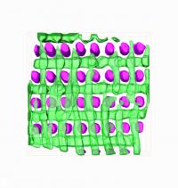 |
| Transmission electron microscope (TEM) tomography provides a nanoscale, 3-D visualization of the structure of a templated block copolymer. The purple features are silica posts fabricated by electron-beam lithography that direct the self-assembly of the copolymer. The material self-assembles to form two orthogonal layers of cylinders (green).
Credit: Winterstein/NIST |
Abstract:
A few short years ago, the idea of a practical manufacturing process based on getting molecules to organize themselves in useful nanoscale shapes seemed ... well, cool, sure, but also a little fantastic. Now the day isn't far off when your cell phone may depend on it. Two recent papers emphasize the point by demonstrating complementary approaches to fine-tuning the key step: depositing thin films of a uniquely designed polymer on a template so that it self-assembles into neat, precise, even rows of alternating composition just 10 or so nanometers wide.
NIST offers electronics industry 2 ways to snoop on self-organizing molecules
Gaithersburg, MD | Posted on October 22nd, 2014The work by researchers at the National Institute of Standards and Technology (NIST), the Massachusetts Institute of Technology, and IBM Almaden Research Center focuses on block copolymers a special class of polymers that under the proper conditions, will segregate on a microscopic scale into regularly spaced "domains" of different chemical composition. The two groups demonstrated ways to observe and measure the shape and dimensions of the polymer rows in three dimensions. The experimental techniques can prove essential in verifying and tuning the computational models used to guide the fabrication process development.
It's old news that the semiconductor industry is starting to run up against physical limits to the decades-long trend of ever-denser integrated chips with smaller and smaller feature sizes, but it hasn't reached bottom yet. Just recently, Intel Corp. announced that it had in production a new generation of chips with a 14-nanometer minimum feature size. That's a little over five times the width of human DNA.
At those dimensions, the problem is creating the multiple masking layers, sort of tiny stencils, needed to define the microscopic patterns on the production wafer. The optical lithography techniques used to create the masks in a process akin to old-school wet photography are simply not capable of reliably reproducing the extremely small, extremely dense patterns. There are tricks you can use such as creating multiple, overlapping masks, but they are very expensive.
Hence the polymers. "The issue in semiconductor lithography is not really making small features�you can do that�but you can't pack them close together," explains NIST materials scientist Alexander Liddle. "Block copolymers take advantage of the fact that if I make small features relatively far apart, I can put the block copolymer on those guiding patterns and sort of fill in the small details." The strategy is called "density multiplication" and the technique, "directed self-assembly."
Block copolymers (BCPs) are a class of materials made by connecting two or more different polymers that, as they anneal, will form predictable, repeating shapes and patterns. With the proper lithographed template, the BCPs in question will form a thin film in a pattern of narrow, alternating stripes of the two polymer compositions. Alternatively, they can be designed so one polymer forms a pattern of posts embedded in the other. Remove one polymer, and in theory, you have a near-perfect pattern for lines spaced 10 to 20 nanometers apart to become, perhaps, part of a transistor array.
If it works. "The biggest problem for the industry is the patterning has to be perfect. There can't be any defects," says NIST materials scientist Joseph Kline. "In both of our projects we're trying to measure the full structure of the pattern. Normally, it's only easy to see the top surface, and what the industry is worried about is that they make a pattern, and it looks okay on the top, but down inside the film, it isn't."
Kline's group, working with IBM, demonstrated a new measurement technique* that uses low-energy or "soft" X rays produced by the Advanced Light Source at Lawrence Berkeley National Labs to probe the structure of the BCP film from multiple angles. Because the film has a regular, repeating structure, the scattering pattern can be interpreted, much as crystallographers do, to reveal the average shapes of the stripes in the film. If a poor match between the materials causes one set of stripes to broaden out at the base, for example, it will show up in the scattering pattern. Their major innovation was to note that although the basic technique was developed using short-wavelength "hard" X rays that have difficulty distinguishing two closely related polymers, much better results can be obtained using longer wavelength X rays that are more sensitive to differences in the molecular structure.**
While X-ray scattering can measure average properties of the films, Liddle's group, working with MIT, developed a method to look, in detail, at individual sections of a film by doing three-dimensional tomography with a transmission electron microscope (TEM).*** Unlike the scattering technique, the TEM tomography can actually image defects in the polymer structure�but only for a small area. The technique can image an area about 500 nanometers across.
Between them, the two techniques can yield detailed data on the performance of a given BCP patterning system. The data, the researchers say, are most valuable for testing and refining computer models. "Our measurements are both fairly time-consuming, so they're not something industry can use on the fab floor," says Kline. "But as they're developing the process, they can use our measurements to get the models right, then they can do a lot of simulations and let the computers figure it out."
"It's just so expensive and time-consuming to test out a new process," agrees Liddle. "But if my model is well validated and I know the model is going to give me accurate results, then I can crank through the simulations quickly. That's a huge factor in the electronics industry."
###
*With the daunting name "resonant critical dimension small angle X-ray scattering" (res-CDSAXS).
**D.F. Sunday, M.R. Hammond, C. Wang, W. Wu, D. Delongchamp, M. Tjio, J. Cheng, J.W. Pitera, R.J. Kline. Determination of the internal morphology of nanostructures patterned by directed self assembly. ACS Nano, 2014, 8 (8), pp 8426-8437 DOI: 10.1021/nn5029289.
***K.W. Gotrik, T. Lam, A.F. Hannon, W. Bai, Y. Ding, J. Winterstein, A. Alexander-Katz, J.A. Liddle, C.A. Ross. 3D TEM Tomography of templated bilayer films of block copolymers. Advanced Functional Materials. Article first published online Oct. 2, 2014 DOI: 10.1002/adfm.201402457.
####
For more information, please click here
Contacts:
Michael Baum
301-975-2763
Copyright © National Institute of Standards and Technology (NIST)
If you have a comment, please Contact us.Issuers of news releases, not 7th Wave, Inc. or Nanotechnology Now, are solely responsible for the accuracy of the content.
Bookmark:


| Related News Press |
News and information
![]() Simulating magnetization in a Heisenberg quantum spin chain April 5th, 2024
Simulating magnetization in a Heisenberg quantum spin chain April 5th, 2024
![]() NRL charters Navy�s quantum inertial navigation path to reduce drift April 5th, 2024
NRL charters Navy�s quantum inertial navigation path to reduce drift April 5th, 2024
![]() Discovery points path to flash-like memory for storing qubits: Rice find could hasten development of nonvolatile quantum memory April 5th, 2024
Discovery points path to flash-like memory for storing qubits: Rice find could hasten development of nonvolatile quantum memory April 5th, 2024
![]() Good as gold - improving infectious disease testing with gold nanoparticles April 5th, 2024
Good as gold - improving infectious disease testing with gold nanoparticles April 5th, 2024
Thin films
![]() Utilizing palladium for addressing contact issues of buried oxide thin film transistors April 5th, 2024
Utilizing palladium for addressing contact issues of buried oxide thin film transistors April 5th, 2024
Imaging
![]() Nanoscale CL thermometry with lanthanide-doped heavy-metal oxide in TEM March 8th, 2024
Nanoscale CL thermometry with lanthanide-doped heavy-metal oxide in TEM March 8th, 2024
Laboratories
![]() A battery�s hopping ions remember where they�ve been: Seen in atomic detail, the seemingly smooth flow of ions through a battery�s electrolyte is surprisingly complicated February 16th, 2024
A battery�s hopping ions remember where they�ve been: Seen in atomic detail, the seemingly smooth flow of ions through a battery�s electrolyte is surprisingly complicated February 16th, 2024
![]() NRL discovers two-dimensional waveguides February 16th, 2024
NRL discovers two-dimensional waveguides February 16th, 2024
Govt.-Legislation/Regulation/Funding/Policy
![]() NRL charters Navy�s quantum inertial navigation path to reduce drift April 5th, 2024
NRL charters Navy�s quantum inertial navigation path to reduce drift April 5th, 2024
![]() Discovery points path to flash-like memory for storing qubits: Rice find could hasten development of nonvolatile quantum memory April 5th, 2024
Discovery points path to flash-like memory for storing qubits: Rice find could hasten development of nonvolatile quantum memory April 5th, 2024
![]() Chemical reactions can scramble quantum information as well as black holes April 5th, 2024
Chemical reactions can scramble quantum information as well as black holes April 5th, 2024
Chip Technology
![]() Discovery points path to flash-like memory for storing qubits: Rice find could hasten development of nonvolatile quantum memory April 5th, 2024
Discovery points path to flash-like memory for storing qubits: Rice find could hasten development of nonvolatile quantum memory April 5th, 2024
![]() Utilizing palladium for addressing contact issues of buried oxide thin film transistors April 5th, 2024
Utilizing palladium for addressing contact issues of buried oxide thin film transistors April 5th, 2024
![]() HKUST researchers develop new integration technique for efficient coupling of III-V and silicon February 16th, 2024
HKUST researchers develop new integration technique for efficient coupling of III-V and silicon February 16th, 2024
Self Assembly
![]() Liquid crystal templated chiral nanomaterials October 14th, 2022
Liquid crystal templated chiral nanomaterials October 14th, 2022
![]() Nanoclusters self-organize into centimeter-scale hierarchical assemblies April 22nd, 2022
Nanoclusters self-organize into centimeter-scale hierarchical assemblies April 22nd, 2022
![]() Atom by atom: building precise smaller nanoparticles with templates March 4th, 2022
Atom by atom: building precise smaller nanoparticles with templates March 4th, 2022
![]() Nanostructures get complex with electron equivalents: Nanoparticles of two different sizes break away from symmetrical designs January 14th, 2022
Nanostructures get complex with electron equivalents: Nanoparticles of two different sizes break away from symmetrical designs January 14th, 2022
Nanoelectronics
![]() Interdisciplinary: Rice team tackles the future of semiconductors Multiferroics could be the key to ultralow-energy computing October 6th, 2023
Interdisciplinary: Rice team tackles the future of semiconductors Multiferroics could be the key to ultralow-energy computing October 6th, 2023
![]() Key element for a scalable quantum computer: Physicists from Forschungszentrum J�lich and RWTH Aachen University demonstrate electron transport on a quantum chip September 23rd, 2022
Key element for a scalable quantum computer: Physicists from Forschungszentrum J�lich and RWTH Aachen University demonstrate electron transport on a quantum chip September 23rd, 2022
![]() Reduced power consumption in semiconductor devices September 23rd, 2022
Reduced power consumption in semiconductor devices September 23rd, 2022
![]() Atomic level deposition to extend Moore�s law and beyond July 15th, 2022
Atomic level deposition to extend Moore�s law and beyond July 15th, 2022
Discoveries
![]() Chemical reactions can scramble quantum information as well as black holes April 5th, 2024
Chemical reactions can scramble quantum information as well as black holes April 5th, 2024
![]() New micromaterial releases nanoparticles that selectively destroy cancer cells April 5th, 2024
New micromaterial releases nanoparticles that selectively destroy cancer cells April 5th, 2024
![]() Utilizing palladium for addressing contact issues of buried oxide thin film transistors April 5th, 2024
Utilizing palladium for addressing contact issues of buried oxide thin film transistors April 5th, 2024
Announcements
![]() NRL charters Navy�s quantum inertial navigation path to reduce drift April 5th, 2024
NRL charters Navy�s quantum inertial navigation path to reduce drift April 5th, 2024
![]() Discovery points path to flash-like memory for storing qubits: Rice find could hasten development of nonvolatile quantum memory April 5th, 2024
Discovery points path to flash-like memory for storing qubits: Rice find could hasten development of nonvolatile quantum memory April 5th, 2024
Interviews/Book Reviews/Essays/Reports/Podcasts/Journals/White papers/Posters
![]() Simulating magnetization in a Heisenberg quantum spin chain April 5th, 2024
Simulating magnetization in a Heisenberg quantum spin chain April 5th, 2024
![]() Discovery points path to flash-like memory for storing qubits: Rice find could hasten development of nonvolatile quantum memory April 5th, 2024
Discovery points path to flash-like memory for storing qubits: Rice find could hasten development of nonvolatile quantum memory April 5th, 2024
Tools
![]() Ferroelectrically modulate the Fermi level of graphene oxide to enhance SERS response November 3rd, 2023
Ferroelectrically modulate the Fermi level of graphene oxide to enhance SERS response November 3rd, 2023
![]() The USTC realizes In situ electron paramagnetic resonance spectroscopy using single nanodiamond sensors November 3rd, 2023
The USTC realizes In situ electron paramagnetic resonance spectroscopy using single nanodiamond sensors November 3rd, 2023
|
|
||
|
|
||
| The latest news from around the world, FREE | ||
|
|
||
|
|
||
| Premium Products | ||
|
|
||
|
Only the news you want to read!
Learn More |
||
|
|
||
|
Full-service, expert consulting
Learn More |
||
|
|
||