Home > Press > Catching the (Invisible) Wave: UC Santa Barbara researchers create a unique semiconductor that manipulates light in the invisible infrared/terahertz range, paving the way for new and enhanced applications
 |
Abstract:
In a feat that may provide a promising array of applications, from energy efficiency to telecommunications to enhanced imaging, researchers at UC Santa Barbara have created a compound semiconductor of nearly perfect quality with embedded nanostructures containing ordered lines of atoms that can manipulate light energy in the mid-infrared range. More efficient solar cells, less risky and higher resolution biological imaging, and the ability to transmit massive amounts of data at higher speeds are only a few applications that this unique semiconductor will be able to support.
Catching the (Invisible) Wave: UC Santa Barbara researchers create a unique semiconductor that manipulates light in the invisible infrared/terahertz range, paving the way for new and enhanced applications
Santa Barbara, CA | Posted on April 11th, 2014"This is a new and exciting field," said Hong Lu, researcher in UCSB's Department of Materials and Department of Electrical and Computer Engineering, and lead author of a study that appears as a cover story of the March issue in the journal Nano Letters, a publication of the American Chemical Society.
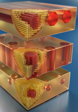
[Right: Artist's concept of nanometer-size metallic wires and metallic particles embedded in semiconductors, as grown by Dr. Hong Lu. Credit: Peter Allen, UCSB]
Key to this technology is the use of erbium, a rare earth metal that has the ability to absorb light in the visible as well as infrared wavelength � which is longer and lower frequency wavelength to which the human eye is accustomed � and has been used for years to enhance the performance of silicon in the production of fiber optics. Pairing erbium with the element antimony (Sb), the researchers embedded the resulting compound � erbium antimonide (ErSb) � as semimetallic nanostructures within the semiconducting matrix of gallium antimonide (GaSb).
ErSb, according to Lu, is an ideal material to match with GaSb because of its structural compatibility with its surrounding material, allowing the researchers to embed the nanostructures without interrupting the atomic lattice structure of the semiconducting matrix. The less flawed the crystal lattice structure of a semiconductor is, the more reliable and better performing the device in which it is used will be.
"The nanostructures are coherently embedded, without introducing noticeable defects, through the growth process by molecular beam epitaxy," said Lu. "Secondly, we can control the size, the shape and the orientation of the nanostructures." The term "epitaxy" refers to a process by which layers of material are deposited atom by atom, or molecule by molecule, one on top of the other with a specific orientation.
"It's really a new kind of heterostructure," said Arthur Gossard, professor in the Materials Department and also in the Department of Electrical and Computer Engineering. While semiconductors incorporating different materials have been studied for years � a technology UCSB professor and Nobel laureate Herbert Kroemer pioneered � a single crystal heterostructured semiconductor/metal is in a class of its own.
The nanostructures allow the compound semiconductor to absorb a wider spectrum of light due to a phenomenon called surface plasmon resonance, said Lu, and that the effect has potential applications in broad research fields, such as solar cells, medical applications to fight cancer, and in the new field of plasmonics.
Optics and electronics operate on vastly different scales, with electron confinement being possible in spaces far smaller than light waves. Therefore, it has been an ongoing challenge for engineers to create a circuit that can take advantage of the speed and data capacity of photons and the compactness of electronics for information processing.
The highly sought bridge between optics and electronics may be found with this compound semiconductor using surface plasmons, electron oscillations at the surface of a metal excited by light. When light (in this case, infrared) hits the surface of this semiconductor, electrons in the nanostructures begin to resonate � that is, move away from their equilibrium positions and oscillate at the same frequency as the infrared light � preserving the optical information, but shrinking it to a scale that would be compatible with electronic devices.
In the realm of imaging, embedded nanowires of ErSb offer a strong broadband polarization effect, according to Lu, filtering and defining images with infrared and even longer-wavelength terahertz light signatures. This effect can be used to image a variety of materials, including the human body, without the risk posed by the higher energies that emanate from X-rays, for instance. Chemicals such as those found in explosives and some illegal narcotics have unique absorption features in this spectrum region. The researchers have already applied for a patent for these embedded nanowires as a broadband light polarizer.
"For infrared imaging, if you can do it with controllable polarizations, there's information there," said Gossard.
While infrared and terahertz wavelengths offer much in the way of the kind of information they can provide, the development of instruments that can take full advantage of their range of frequencies is still an emerging field. Lu credits this breakthrough to the collaborative nature of the research on the UCSB campus, which allowed her to merge her materials expertise with the skills of researchers who specialize in infrared and terahertz technology.
"It's amazing here," she said. "We basically collaborated and discovered all these interesting features and properties of the material together."
"One of the most exciting things about this for me is that this was a �grassroots' collaboration," said Mark Sherwin, professor of physics, director of the Institute for Terahertz Science and Technology at UCSB, and one of the paper's co-authors. The idea for the direction of the research came from the junior researchers in the group, he said, grad students and undergrads from different laboratories and research groups working on different aspects of the project, all of whom decided to combine their efforts and their expertise into one study. "I think what's really special about UCSB is that we can have an environment like that."
Since the paper was written, most of the researchers have gone into industry: Daniel G. Ouelette and Benjamin Zaks, formerly of the Department of Physics and the Institute for Terahertz Science and Technology at UCSB, now work at Intel and Agilent, respectively. Their colleague Justin Watts, who was an undergraduate participant is now pursuing graduate studies at the University of Minnesota. Peter Burke, formerly of the UCSB Materials Department, now works at Lockheed Martin. Sascha Preu, a former postdoc in the Sherwin Group, is now assistant professor at the Technical University of Darmstadt.
Researchers on campus are also exploring the possibilities of this technology in the field of thermoelectrics, which studies how temperature differences of a material can create electric voltage or how differences in electric voltages in a material can create temperature differences. Renowned UCSB researchers John Bowers (solid state photonics) and Christopher Palmstrom (heteroepitaxial growth of novel materials) are investigating the potential of this new semiconductor.
Author: Sonia Fernandez, UCSB Public Affairs
####
For more information, please click here
Contacts:
Melissa Van De Werfhorst
Copyright © University of California - Santa Barbara
If you have a comment, please Contact us.Issuers of news releases, not 7th Wave, Inc. or Nanotechnology Now, are solely responsible for the accuracy of the content.
Bookmark:


| Related Links |
| Related News Press |
News and information
![]() Simulating magnetization in a Heisenberg quantum spin chain April 5th, 2024
Simulating magnetization in a Heisenberg quantum spin chain April 5th, 2024
![]() NRL charters Navy�s quantum inertial navigation path to reduce drift April 5th, 2024
NRL charters Navy�s quantum inertial navigation path to reduce drift April 5th, 2024
![]() Discovery points path to flash-like memory for storing qubits: Rice find could hasten development of nonvolatile quantum memory April 5th, 2024
Discovery points path to flash-like memory for storing qubits: Rice find could hasten development of nonvolatile quantum memory April 5th, 2024
Imaging
![]() Nanoscale CL thermometry with lanthanide-doped heavy-metal oxide in TEM March 8th, 2024
Nanoscale CL thermometry with lanthanide-doped heavy-metal oxide in TEM March 8th, 2024
![]() The USTC realizes In situ electron paramagnetic resonance spectroscopy using single nanodiamond sensors November 3rd, 2023
The USTC realizes In situ electron paramagnetic resonance spectroscopy using single nanodiamond sensors November 3rd, 2023
Wireless/telecommunications/RF/Antennas/Microwaves
![]() HKUST researchers develop new integration technique for efficient coupling of III-V and silicon February 16th, 2024
HKUST researchers develop new integration technique for efficient coupling of III-V and silicon February 16th, 2024
Nanoelectronics
![]() Interdisciplinary: Rice team tackles the future of semiconductors Multiferroics could be the key to ultralow-energy computing October 6th, 2023
Interdisciplinary: Rice team tackles the future of semiconductors Multiferroics could be the key to ultralow-energy computing October 6th, 2023
![]() Key element for a scalable quantum computer: Physicists from Forschungszentrum J�lich and RWTH Aachen University demonstrate electron transport on a quantum chip September 23rd, 2022
Key element for a scalable quantum computer: Physicists from Forschungszentrum J�lich and RWTH Aachen University demonstrate electron transport on a quantum chip September 23rd, 2022
![]() Reduced power consumption in semiconductor devices September 23rd, 2022
Reduced power consumption in semiconductor devices September 23rd, 2022
![]() Atomic level deposition to extend Moore�s law and beyond July 15th, 2022
Atomic level deposition to extend Moore�s law and beyond July 15th, 2022
Discoveries
![]() Chemical reactions can scramble quantum information as well as black holes April 5th, 2024
Chemical reactions can scramble quantum information as well as black holes April 5th, 2024
![]() New micromaterial releases nanoparticles that selectively destroy cancer cells April 5th, 2024
New micromaterial releases nanoparticles that selectively destroy cancer cells April 5th, 2024
![]() Utilizing palladium for addressing contact issues of buried oxide thin film transistors April 5th, 2024
Utilizing palladium for addressing contact issues of buried oxide thin film transistors April 5th, 2024
Announcements
![]() NRL charters Navy�s quantum inertial navigation path to reduce drift April 5th, 2024
NRL charters Navy�s quantum inertial navigation path to reduce drift April 5th, 2024
![]() Discovery points path to flash-like memory for storing qubits: Rice find could hasten development of nonvolatile quantum memory April 5th, 2024
Discovery points path to flash-like memory for storing qubits: Rice find could hasten development of nonvolatile quantum memory April 5th, 2024
Interviews/Book Reviews/Essays/Reports/Podcasts/Journals/White papers/Posters
![]() Simulating magnetization in a Heisenberg quantum spin chain April 5th, 2024
Simulating magnetization in a Heisenberg quantum spin chain April 5th, 2024
![]() Discovery points path to flash-like memory for storing qubits: Rice find could hasten development of nonvolatile quantum memory April 5th, 2024
Discovery points path to flash-like memory for storing qubits: Rice find could hasten development of nonvolatile quantum memory April 5th, 2024
Tools
![]() Ferroelectrically modulate the Fermi level of graphene oxide to enhance SERS response November 3rd, 2023
Ferroelectrically modulate the Fermi level of graphene oxide to enhance SERS response November 3rd, 2023
![]() The USTC realizes In situ electron paramagnetic resonance spectroscopy using single nanodiamond sensors November 3rd, 2023
The USTC realizes In situ electron paramagnetic resonance spectroscopy using single nanodiamond sensors November 3rd, 2023
Energy
![]() Development of zinc oxide nanopagoda array photoelectrode: photoelectrochemical water-splitting hydrogen production January 12th, 2024
Development of zinc oxide nanopagoda array photoelectrode: photoelectrochemical water-splitting hydrogen production January 12th, 2024
![]() Shedding light on unique conduction mechanisms in a new type of perovskite oxide November 17th, 2023
Shedding light on unique conduction mechanisms in a new type of perovskite oxide November 17th, 2023
![]() Inverted perovskite solar cell breaks 25% efficiency record: Researchers improve cell efficiency using a combination of molecules to address different November 17th, 2023
Inverted perovskite solar cell breaks 25% efficiency record: Researchers improve cell efficiency using a combination of molecules to address different November 17th, 2023
![]() The efficient perovskite cells with a structured anti-reflective layer � another step towards commercialization on a wider scale October 6th, 2023
The efficient perovskite cells with a structured anti-reflective layer � another step towards commercialization on a wider scale October 6th, 2023
Battery Technology/Capacitors/Generators/Piezoelectrics/Thermoelectrics/Energy storage
![]() What heat can tell us about battery chemistry: using the Peltier effect to study lithium-ion cells March 8th, 2024
What heat can tell us about battery chemistry: using the Peltier effect to study lithium-ion cells March 8th, 2024
![]() A battery�s hopping ions remember where they�ve been: Seen in atomic detail, the seemingly smooth flow of ions through a battery�s electrolyte is surprisingly complicated February 16th, 2024
A battery�s hopping ions remember where they�ve been: Seen in atomic detail, the seemingly smooth flow of ions through a battery�s electrolyte is surprisingly complicated February 16th, 2024
Solar/Photovoltaic
![]() Development of zinc oxide nanopagoda array photoelectrode: photoelectrochemical water-splitting hydrogen production January 12th, 2024
Development of zinc oxide nanopagoda array photoelectrode: photoelectrochemical water-splitting hydrogen production January 12th, 2024
![]() Shedding light on unique conduction mechanisms in a new type of perovskite oxide November 17th, 2023
Shedding light on unique conduction mechanisms in a new type of perovskite oxide November 17th, 2023
![]() Inverted perovskite solar cell breaks 25% efficiency record: Researchers improve cell efficiency using a combination of molecules to address different November 17th, 2023
Inverted perovskite solar cell breaks 25% efficiency record: Researchers improve cell efficiency using a combination of molecules to address different November 17th, 2023
![]() Charged �molecular beasts� the basis for new compounds: Researchers at Leipzig University use �aggressive� fragments of molecular ions for chemical synthesis November 3rd, 2023
Charged �molecular beasts� the basis for new compounds: Researchers at Leipzig University use �aggressive� fragments of molecular ions for chemical synthesis November 3rd, 2023
|
|
||
|
|
||
| The latest news from around the world, FREE | ||
|
|
||
|
|
||
| Premium Products | ||
|
|
||
|
Only the news you want to read!
Learn More |
||
|
|
||
|
Full-service, expert consulting
Learn More |
||
|
|
||