Home > Press > Bruker Launches ContourSP 3D Optical Microscope for PCB Industry: Large-Format Metrology System Debuts to Over $5 Million in Orders
 |
Abstract:
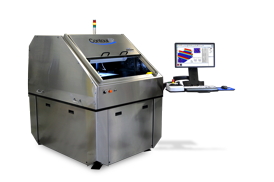
Bruker announced today that it has launched the ContourSP large panel metrology system, which more than doubles the measurement throughput of the high-density interconnect (HDI) substrates in multi-chip modules (MCM) over previous generation SP models used by the semiconductor packaging industry. Specifically designed to measure each layer of the printed circuit board (PCB) panels during manufacturing, the gage-capable ContourSP assures the minimum recipe development time, highest yield, maximum up-time, and lowest cost per measured panel in production. These features have already led to over $5 million in orders by several leading HDI/MCM PCB manufacturers.
Bruker Launches ContourSP 3D Optical Microscope for PCB Industry: Large-Format Metrology System Debuts to Over $5 Million in Orders
Tucson, AZ | Posted on December 10th, 2013"Demand for Bruker's fifth generation SP model continues to build as early adoption customers enjoy the advanced capabilities and ease of use offered by the ContourSP," said Mark R. Munch, Ph.D., President of the Bruker MAT Group. "By doubling the throughput and adding new proprietary measurement capabilities, our customers are able to achieve maximum productivity in this era of ever smaller line widths and tighter tolerances in the PCB industry."
"Not only is the ContourSP much faster than other systems at performing these precise measurements, but we've added a number of productivity enhancing features," added Kent Heath, Senior Director of Marketing for Bruker's Stylus and Optical Business. "The new Vision64� operator interface with multi-processing features multi-region analysis, automatic re-measurement, and our proprietary Dynamic Signal Segmentation (DSS) analysis, making the ContourSP the most comprehensive tool available."
About ContourSP
Based on white light interferometry, the ContourSP incorporates decades of packaging and panel measurement experience to provide unprecedented speed, metrology capability, reliability, serviceability, and manufacturing readiness for 3D critical dimension measurements in MCM and HDI PCB applications. Bruker's high-performance 3D optical microscopes feature Vision64 operating and analysis software, and the industry's most intuitive, modular user interface to deliver user-level-customization capabilities for the widest possible range of surface profiling metrology applications. The ContourSP also utilizes Bruker's revolutionary gantry-based design and integrated workstation to support up to 600x600-millimeter samples in a highly compact footprint.
####
About Bruker Corporation
Bruker Corporation is a leading provider of high-performance scientific instruments and solutions for molecular and materials research, as well as for industrial and applied analysis.
For more information, please click here
Contacts:
Stephen Hopkins, Marketing Communications
Bruker Nano Surfaces Division
3400 East Britannia Drive, Suite 150, Tucson, AZ 85706
T: +1 (520) 741-1044 x1022
Copyright © Bruker Corporation
If you have a comment, please Contact us.Issuers of news releases, not 7th Wave, Inc. or Nanotechnology Now, are solely responsible for the accuracy of the content.
Bookmark:


| Related News Press |
News and information
![]() Simulating magnetization in a Heisenberg quantum spin chain April 5th, 2024
Simulating magnetization in a Heisenberg quantum spin chain April 5th, 2024
![]() NRL charters Navy�s quantum inertial navigation path to reduce drift April 5th, 2024
NRL charters Navy�s quantum inertial navigation path to reduce drift April 5th, 2024
![]() Discovery points path to flash-like memory for storing qubits: Rice find could hasten development of nonvolatile quantum memory April 5th, 2024
Discovery points path to flash-like memory for storing qubits: Rice find could hasten development of nonvolatile quantum memory April 5th, 2024
Imaging
![]() Nanoscale CL thermometry with lanthanide-doped heavy-metal oxide in TEM March 8th, 2024
Nanoscale CL thermometry with lanthanide-doped heavy-metal oxide in TEM March 8th, 2024
![]() The USTC realizes In situ electron paramagnetic resonance spectroscopy using single nanodiamond sensors November 3rd, 2023
The USTC realizes In situ electron paramagnetic resonance spectroscopy using single nanodiamond sensors November 3rd, 2023
![]() Observation of left and right at nanoscale with optical force October 6th, 2023
Observation of left and right at nanoscale with optical force October 6th, 2023
Chip Technology
![]() Discovery points path to flash-like memory for storing qubits: Rice find could hasten development of nonvolatile quantum memory April 5th, 2024
Discovery points path to flash-like memory for storing qubits: Rice find could hasten development of nonvolatile quantum memory April 5th, 2024
![]() Utilizing palladium for addressing contact issues of buried oxide thin film transistors April 5th, 2024
Utilizing palladium for addressing contact issues of buried oxide thin film transistors April 5th, 2024
![]() HKUST researchers develop new integration technique for efficient coupling of III-V and silicon February 16th, 2024
HKUST researchers develop new integration technique for efficient coupling of III-V and silicon February 16th, 2024
Announcements
![]() NRL charters Navy�s quantum inertial navigation path to reduce drift April 5th, 2024
NRL charters Navy�s quantum inertial navigation path to reduce drift April 5th, 2024
![]() Discovery points path to flash-like memory for storing qubits: Rice find could hasten development of nonvolatile quantum memory April 5th, 2024
Discovery points path to flash-like memory for storing qubits: Rice find could hasten development of nonvolatile quantum memory April 5th, 2024
New-Contracts/Sales/Customers
![]() Bruker Light-Sheet Microscopes at Major Comprehensive Cancer Center: New Advanced Imaging Center Powered by Two MuVi and LCS SPIM Microscopes March 25th, 2021
Bruker Light-Sheet Microscopes at Major Comprehensive Cancer Center: New Advanced Imaging Center Powered by Two MuVi and LCS SPIM Microscopes March 25th, 2021
![]() Arrowhead Pharmaceuticals Announces Closing of Agreement with Takeda November 27th, 2020
Arrowhead Pharmaceuticals Announces Closing of Agreement with Takeda November 27th, 2020
![]() Veeco Announces Aledia Order of 300mm MOCVD Equipment for microLED Displays: Propel� Platform First 300mm System with EFEM Designed for Advanced Display Applications October 20th, 2020
Veeco Announces Aledia Order of 300mm MOCVD Equipment for microLED Displays: Propel� Platform First 300mm System with EFEM Designed for Advanced Display Applications October 20th, 2020
![]() GREENWAVES TECHNOLOGIES Announces Next Generation GAP9 Hearables Platform Using GLOBALFOUNDRIES 22FDX Solution October 16th, 2020
GREENWAVES TECHNOLOGIES Announces Next Generation GAP9 Hearables Platform Using GLOBALFOUNDRIES 22FDX Solution October 16th, 2020
|
|
||
|
|
||
| The latest news from around the world, FREE | ||
|
|
||
|
|
||
| Premium Products | ||
|
|
||
|
Only the news you want to read!
Learn More |
||
|
|
||
|
Full-service, expert consulting
Learn More |
||
|
|
||