Home > Press > How Graphene’s Electrical Properties Can Be Tuned: Fortuitous discovery in UC Riverside physics lab made using stacked layers of “wonder material”
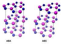 |
| In Bernal-stacked trilayer (ABA), the top (third) sheet is exactly on top of the lowest sheet. In rhombohedral-stacked (ABC) trilayer, the top sheet is shifted by the distance of an atom, so that the top (third) sheet and the lowest sheet form a Bernal stacking as well. Photo credit: Lau lab, UC Riverside. |
Abstract:
An accidental discovery in a physicist's laboratory at the University of California, Riverside provides a unique route for tuning the electrical properties of graphene, nature's thinnest elastic material. This route holds great promise for replacing silicon with graphene in the microchip industry.
How Graphene’s Electrical Properties Can Be Tuned: Fortuitous discovery in UC Riverside physics lab made using stacked layers of “wonder material”
Riverside, CA | Posted on September 26th, 2011The researchers found that stacking up three layers of graphene, like pancakes, significantly modifies the material's electrical properties. When they fabricated trilayer graphene in the lab and measured its conductance, they found, to their surprise, that depending on how the layers were stacked some of the trilayer graphene devices were conducting while others were insulating.
"What we stumbled upon is a simple and convenient ‘knob' for tuning graphene sheets' electrical properties," said Jeanie Lau, an associate professor of physics and astronomy, whose lab made the serendipitous finding.
Study results appeared online Sept. 25 in Nature Physics.
Graphene is a one-atom thick sheet of carbon atoms arranged in hexagonal rings. Bearing excellent material properties, such as high current-carrying capacity and thermal conductivity, this "wonder material" is ideally suited for creating components for semiconductor circuits and computers.
Because of the planar and chicken wire-like structure of graphene, its sheets lend themselves well to stacking in what is called ‘Bernal stacking,' the stacking fashion of graphene sheets.
In a Bernal-stacked bilayer, one corner of the hexagons of the second sheet is located above the center of the hexagons of the bottom sheet. In Bernal-stacked trilayer (ABA), the top (third) sheet is exactly on top of the lowest sheet. In rhombohedral-stacked (ABC) trilayer, the top sheet is shifted by the distance of an atom, so that the top (third) sheet and the lowest sheet form a Bernal stacking as well.
"The most stable form of trilayer graphene is ABA, which behaves like a metal," Lau explained. "Amazingly, if we simply shift the entire topmost layer by the distance of a single atom, the trilayer - now with ABC or rhombohedral stacking - becomes insulating. Why this happens is not clear as yet. It could be induced by electronic interactions. We eagerly await an explanation from theorists!"
Her lab used Raman spectroscopy to examine the graphene devices' stacking orders. Next the lab plans to investigate the nature of the insulating state in ABC-stacked graphene. In this kind of stacked graphene, they also plan to study the band gap - a range in energy, critical for digital applications, in which no electrons can exist.
"The presence of the gap in ABC-stacked graphene that arises, we believe, from enhanced electronic interactions is interesting since it is not expected from theoretical calculations," Lau said. "Understanding this gap is particularly important for the major challenge of band gap engineering in graphene electronics."
Besides graphene, Lau studies nanowires and carbon nanotubes. Her research has helped physicists gain fundamental understanding of how atoms and electrons behave when they are ruled by quantum mechanics. Her lab studies novel electrical properties that arise from the quantum confinement of atoms and charges to nanoscale systems. Her research team has shown that graphene can act as an atomic-scale billiard table, with electric charges acting as billiard balls.
Her other research interests include superconductivity, thermal management and electronic transport in nanostructures, and engineering new classes of nanoscale devices.
An educational component of Lau's research effort is the active involvement of high school, undergraduate, and graduate students, especially minority and women, in her cutting-edge research, taking advantage of the ethnic diversity of UCR's student population and local communities. She is a founding faculty member of the UCR Undergraduate Research Journal. She also organized a "Women in Physics" lunch group that provides a friendly platform for female students, postdocs and faculty members to interact.
After receiving her bachelor's degree in physics from the University of Chicago in 1994, Lau proceeded to Harvard University from where she received her master's and doctoral degrees in physics in 1997 and 2001, respectively. She joined UCR in 2004, after an appointment as a research associate in the Hewlett-Packard Laboratory.
Lau's awards and honors include a Presidential Early Career Award for Scientists and Engineers, 2009; a National Science Foundation CAREER Award, 2008; the Richter Fellowship for Undergraduate Research, 1992; a David W. Grainger Senior Scholarship, 1993; and a Robert T. Poe Faculty Development Grant from the Chinese-American Faculty Association of Southern California, 2007. She has published more than 60 research articles in peer-reviewed journals.
Lau, a member of UCR's Center for Nanoscale Science and Engineering, was joined in the research by W. Bao (the first author of the research paper), L. Jing, J. Velasco Jr., Y. Lee, G. Liu, D. Tran and M. Bockrath at UCR; B. Stanley at Caltech; M. Aykol and S. B. Cronin at the University of Southern California; D. Smirnov at the National High Magnetic Field Laboratory, Fla.; M. Koshino at Tohoku University, Japan; and E. McCann at Lancaster University, United Kingdom.
The research was funded by grants from the National Science Foundation, Office of Naval Research, and the Focus Center for Functional Engineered Nano Architectonics.
####
About University of California, Riverside
The University of California, Riverside (www.ucr.edu) is a doctoral research university, a living laboratory for groundbreaking exploration of issues critical to Inland Southern California, the state and communities around the world. Reflecting California's diverse culture, UCR's enrollment has exceeded 20,500 students. The campus will open a medical school in 2013 and has reached the heart of the Coachella Valley by way of the UCR Palm Desert Graduate Center. The campus has an annual statewide economic impact of more than $1 billion.
For more information, please click here
Contacts:
Iqbal Pittalwala
Tel: (951) 827-6050
Jeanie Lau
Copyright © University of California, Riverside
If you have a comment, please Contact us.Issuers of news releases, not 7th Wave, Inc. or Nanotechnology Now, are solely responsible for the accuracy of the content.
Bookmark:


| Related Links |
![]() Department of Physics and Astronomy:
Department of Physics and Astronomy:
![]() Center for Nanoscale Science and Engineering:
Center for Nanoscale Science and Engineering:
| Related News Press |
News and information
![]() Simulating magnetization in a Heisenberg quantum spin chain April 5th, 2024
Simulating magnetization in a Heisenberg quantum spin chain April 5th, 2024
![]() NRL charters Navy’s quantum inertial navigation path to reduce drift April 5th, 2024
NRL charters Navy’s quantum inertial navigation path to reduce drift April 5th, 2024
![]() Discovery points path to flash-like memory for storing qubits: Rice find could hasten development of nonvolatile quantum memory April 5th, 2024
Discovery points path to flash-like memory for storing qubits: Rice find could hasten development of nonvolatile quantum memory April 5th, 2024
Graphene/ Graphite
![]() NRL discovers two-dimensional waveguides February 16th, 2024
NRL discovers two-dimensional waveguides February 16th, 2024
Chip Technology
![]() Discovery points path to flash-like memory for storing qubits: Rice find could hasten development of nonvolatile quantum memory April 5th, 2024
Discovery points path to flash-like memory for storing qubits: Rice find could hasten development of nonvolatile quantum memory April 5th, 2024
![]() Utilizing palladium for addressing contact issues of buried oxide thin film transistors April 5th, 2024
Utilizing palladium for addressing contact issues of buried oxide thin film transistors April 5th, 2024
![]() HKUST researchers develop new integration technique for efficient coupling of III-V and silicon February 16th, 2024
HKUST researchers develop new integration technique for efficient coupling of III-V and silicon February 16th, 2024
Nanotubes/Buckyballs/Fullerenes/Nanorods/Nanostrings
![]() Tests find no free-standing nanotubes released from tire tread wear September 8th, 2023
Tests find no free-standing nanotubes released from tire tread wear September 8th, 2023
![]() Detection of bacteria and viruses with fluorescent nanotubes July 21st, 2023
Detection of bacteria and viruses with fluorescent nanotubes July 21st, 2023
Nanoelectronics
![]() Interdisciplinary: Rice team tackles the future of semiconductors Multiferroics could be the key to ultralow-energy computing October 6th, 2023
Interdisciplinary: Rice team tackles the future of semiconductors Multiferroics could be the key to ultralow-energy computing October 6th, 2023
![]() Key element for a scalable quantum computer: Physicists from Forschungszentrum Jülich and RWTH Aachen University demonstrate electron transport on a quantum chip September 23rd, 2022
Key element for a scalable quantum computer: Physicists from Forschungszentrum Jülich and RWTH Aachen University demonstrate electron transport on a quantum chip September 23rd, 2022
![]() Reduced power consumption in semiconductor devices September 23rd, 2022
Reduced power consumption in semiconductor devices September 23rd, 2022
![]() Atomic level deposition to extend Moore’s law and beyond July 15th, 2022
Atomic level deposition to extend Moore’s law and beyond July 15th, 2022
Discoveries
![]() Chemical reactions can scramble quantum information as well as black holes April 5th, 2024
Chemical reactions can scramble quantum information as well as black holes April 5th, 2024
![]() New micromaterial releases nanoparticles that selectively destroy cancer cells April 5th, 2024
New micromaterial releases nanoparticles that selectively destroy cancer cells April 5th, 2024
![]() Utilizing palladium for addressing contact issues of buried oxide thin film transistors April 5th, 2024
Utilizing palladium for addressing contact issues of buried oxide thin film transistors April 5th, 2024
Announcements
![]() NRL charters Navy’s quantum inertial navigation path to reduce drift April 5th, 2024
NRL charters Navy’s quantum inertial navigation path to reduce drift April 5th, 2024
![]() Discovery points path to flash-like memory for storing qubits: Rice find could hasten development of nonvolatile quantum memory April 5th, 2024
Discovery points path to flash-like memory for storing qubits: Rice find could hasten development of nonvolatile quantum memory April 5th, 2024
Grants/Sponsored Research/Awards/Scholarships/Gifts/Contests/Honors/Records
![]() Discovery points path to flash-like memory for storing qubits: Rice find could hasten development of nonvolatile quantum memory April 5th, 2024
Discovery points path to flash-like memory for storing qubits: Rice find could hasten development of nonvolatile quantum memory April 5th, 2024
![]() Chemical reactions can scramble quantum information as well as black holes April 5th, 2024
Chemical reactions can scramble quantum information as well as black holes April 5th, 2024
|
|
||
|
|
||
| The latest news from around the world, FREE | ||
|
|
||
|
|
||
| Premium Products | ||
|
|
||
|
Only the news you want to read!
Learn More |
||
|
|
||
|
Full-service, expert consulting
Learn More |
||
|
|
||