Home > Press > Nanotechnology Students Make World's Smallest Images of Stephen Colbert
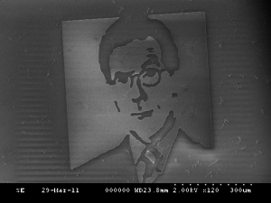 |
| The smallest likeness of Stephen Colbert in the world, "Micro Colbert". Four micro sized images of Stephen were fabricated in a clean room environment on a silicon wafer by two nanotech undergrad students at the University of Waterloo. |
Abstract:
The world's smallest images of Stephen Colbert were made by two undergraduate nanotechnology engineering students. John Maier and Erin Bedford fabricated four micro sized images of Stephen Colbert in a clean room at the University of Waterloo.
Nanotechnology Students Make World's Smallest Images of Stephen Colbert
Waterloo, Canada | Posted on April 6th, 2011The world's smallest images of Stephen Colbert were made by two undergraduate nanotechnology engineering students. The students, John Maier and Erin Bedford, fabricated four micro sized images of Stephen Colbert (www.microcolbert.com). The two students are graduating from the Nanotechnology Engineering program at the University of Waterloo. The smallest of the four images measured approximately 110μm by 130μm, while the largest measured 1.8mm by 2.3mm. The smallest feature size on the smallest image measured approximately 400nm across. Images were captured of each Colbert image using a Scanning Electron Microscope (SEM). The Micro Colbert images were made from a micrometer thin layer of aluminum that was sputtered on to the substrate through a photoresist pattern.
A layer of chrome metal was deposited on a blank wafer followed by a silicon nitride (SiN) layer, grown using plasma-enhanced chemical vapor deposition (PECVD). The SiN layer was then dry etched using reactive-ion etching (RIE). A layer of aluminum was then deposited on the wafer using sputtering and treated, completing the wafer fabrication. Lithography techniques were used throughout the process to generate the designed patterns.
John Maier (www.johnmaier.com) and Erin Bedford (ca.linkedin.com/pub/erin-bedford/16/2b4/614) are part of the second graduating class of the new Nanotechnology Engineering program at the University of Waterloo. "Hopefully Stephen will cover it on the show and help to get kids excited about nanotechnology," John said. During the course of their co-op degree, Erin has interned at the University of Albany, Xerox Research Center of Canada and EMPA in Switzerland. John has interned at Broadcom Corporation, the National Research Council of Canada and Facebook.
For more information on Micro Colbert please visit the website www.microcolbert.com, or follow the pages on Facebook or Twitter.
####
For more information, please click here
Contacts:
John Maier
Copyright © John Maier
If you have a comment, please Contact us.Issuers of news releases, not 7th Wave, Inc. or Nanotechnology Now, are solely responsible for the accuracy of the content.
Bookmark:


| Related News Press |
News and information
![]() Quantum computer improves AI predictions April 17th, 2026
Quantum computer improves AI predictions April 17th, 2026
![]() Flexible sensor gains sensitivity under pressure April 17th, 2026
Flexible sensor gains sensitivity under pressure April 17th, 2026
![]() A reusable chip for particulate matter sensing April 17th, 2026
A reusable chip for particulate matter sensing April 17th, 2026
![]() Detecting vibrational quantum beating in the predissociation dynamics of SF6 using time-resolved photoelectron spectroscopy April 17th, 2026
Detecting vibrational quantum beating in the predissociation dynamics of SF6 using time-resolved photoelectron spectroscopy April 17th, 2026
Imaging
![]() Simple algorithm paired with standard imaging tool could predict failure in lithium metal batteries August 8th, 2025
Simple algorithm paired with standard imaging tool could predict failure in lithium metal batteries August 8th, 2025
Chip Technology
![]() A reusable chip for particulate matter sensing April 17th, 2026
A reusable chip for particulate matter sensing April 17th, 2026
![]() Metasurfaces smooth light to boost magnetic sensing precision January 30th, 2026
Metasurfaces smooth light to boost magnetic sensing precision January 30th, 2026
Announcements
![]() A fundamentally new therapeutic approach to cystic fibrosis: Nanobody repairs cellular defect April 17th, 2026
A fundamentally new therapeutic approach to cystic fibrosis: Nanobody repairs cellular defect April 17th, 2026
![]() UC Irvine physicists discover method to reverse �quantum scrambling� : The work addresses the problem of information loss in quantum computing system April 17th, 2026
UC Irvine physicists discover method to reverse �quantum scrambling� : The work addresses the problem of information loss in quantum computing system April 17th, 2026
Human Interest/Art
![]() New 2D multifractal tools delve into Pollock's expressionism January 17th, 2025
New 2D multifractal tools delve into Pollock's expressionism January 17th, 2025
![]() Drawing data in nanometer scale September 30th, 2022
Drawing data in nanometer scale September 30th, 2022
![]() Scientists prepare for the world�s smallest race: Nanocar Race II March 18th, 2022
Scientists prepare for the world�s smallest race: Nanocar Race II March 18th, 2022
![]() Graphene nanotubes revolutionize touch screen use for prosthetic hands August 3rd, 2021
Graphene nanotubes revolutionize touch screen use for prosthetic hands August 3rd, 2021
Printing/Lithography/Inkjet/Inks/Bio-printing/Dyes
![]() Presenting: Ultrasound-based printing of 3D materials�potentially inside the body December 8th, 2023
Presenting: Ultrasound-based printing of 3D materials�potentially inside the body December 8th, 2023
![]() Simple ballpoint pen can write custom LEDs August 11th, 2023
Simple ballpoint pen can write custom LEDs August 11th, 2023
![]() Disposable electronics on a simple sheet of paper October 7th, 2022
Disposable electronics on a simple sheet of paper October 7th, 2022
|
|
||
|
|
||
| The latest news from around the world, FREE | ||
|
|
||
|
|
||
| Premium Products | ||
|
|
||
|
Only the news you want to read!
Learn More |
||
|
|
||
|
Full-service, expert consulting
Learn More |
||
|
|
||