Home > Press > New transistors: An alternative to silicon and better than graphene
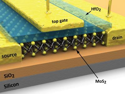 |
| This is a digital model showing how molybdenite can be integrated into a transistor. Credit: Credit: EPFL |
Abstract:
Smaller and more energy-efficient electronic chips could be made using molybdenite. In an article appearing online January 30 in the journal Nature Nanotechnology, EPFL's Laboratory of Nanoscale Electronics and Structures (LANES) publishes a study showing that this material has distinct advantages over traditional silicon or graphene for use in electronics applications.
New transistors: An alternative to silicon and better than graphene
France | Posted on January 30th, 2011A discovery made at EPFL could play an important role in electronics, allowing us to make transistors that are smaller and more energy efficient. Research carried out in the Laboratory of Nanoscale Electronics and Structures (LANES) has revealed that molybdenite, or MoS2, is a very effective semiconductor. This mineral, which is abundant in nature, is often used as an element in steel alloys or as an additive in lubricants. But it had not yet been extensively studied for use in electronics.
100,000 times less energy
"It's a two-dimensional material, very thin and easy to use in nanotechnology. It has real potential in the fabrication of very small transistors, light-emitting diodes (LEDs) and solar cells," says EPFL Professor Andras Kis, whose LANES colleagues M. Radisavljevic, Prof. Radenovic et M. Brivio worked with him on the study. He compares its advantages with two other materials: silicon, currently the primary component used in electronic and computer chips, and graphene, whose discovery in 2004 earned University of Manchester physicists Andr� Geim and Konstantin Novoselov the 2010 Nobel Prize in Physics.
One of molybdenite's advantages is that it is less voluminous than silicon, which is a three-dimensional material. "In a 0.65-nanometer-thick sheet of MoS2, the electrons can move around as easily as in a 2-nanometer-thick sheet of silicon," explains Kis. "But it's not currently possible to fabricate a sheet of silicon as thin as a monolayer sheet of MoS2." Another advantage of molybdenite is that it can be used to make transistors that consume 100,000 times less energy in standby state than traditional silicon transistors. A semi-conductor with a "gap" must be used to turn a transistor on and off, and molybdenite's 1.8 electron-volt gap is ideal for this purpose.
Better than graphene
In solid-state physics, band theory is a way of representing the energy of electrons in a given material. In semi-conductors, electron-free spaces exist between these bands, the so-called "band gaps." If the gap is not too small or too large, certain electrons can hop across the gap. It thus offers a greater level of control over the electrical behavior of the material, which can be turned on and off easily.
The existence of this gap in molybdenite also gives it an advantage over graphene. Considered today by many scientists as the electronics material of the future, the "semi-metal" graphene doesn't have a gap, and it is very difficult to artificially reproduce one in the material.
Direct link to the article: dx.doi.org/10.1038/nnano.2010.279
Contact: Professor Andras Kis, Laboratory of Nanoscale Electronics and Structures (LANES), tel: +41 21 693 39 25
####
For more information, please click here
Contacts:
Michael Mitchell
41-798-103-107
Copyright © Ecole Polytechnique F�d�rale de Lausanne
If you have a comment, please Contact us.Issuers of news releases, not 7th Wave, Inc. or Nanotechnology Now, are solely responsible for the accuracy of the content.
Bookmark:


| Related News Press |
News and information
![]() Simulating magnetization in a Heisenberg quantum spin chain April 5th, 2024
Simulating magnetization in a Heisenberg quantum spin chain April 5th, 2024
![]() NRL charters Navy�s quantum inertial navigation path to reduce drift April 5th, 2024
NRL charters Navy�s quantum inertial navigation path to reduce drift April 5th, 2024
![]() Discovery points path to flash-like memory for storing qubits: Rice find could hasten development of nonvolatile quantum memory April 5th, 2024
Discovery points path to flash-like memory for storing qubits: Rice find could hasten development of nonvolatile quantum memory April 5th, 2024
Possible Futures
![]() Discovery points path to flash-like memory for storing qubits: Rice find could hasten development of nonvolatile quantum memory April 5th, 2024
Discovery points path to flash-like memory for storing qubits: Rice find could hasten development of nonvolatile quantum memory April 5th, 2024
![]() With VECSELs towards the quantum internet Fraunhofer: IAF achieves record output power with VECSEL for quantum frequency converters April 5th, 2024
With VECSELs towards the quantum internet Fraunhofer: IAF achieves record output power with VECSEL for quantum frequency converters April 5th, 2024
Academic/Education
![]() Rice University launches Rice Synthetic Biology Institute to improve lives January 12th, 2024
Rice University launches Rice Synthetic Biology Institute to improve lives January 12th, 2024
![]() Multi-institution, $4.6 million NSF grant to fund nanotechnology training September 9th, 2022
Multi-institution, $4.6 million NSF grant to fund nanotechnology training September 9th, 2022
Chip Technology
![]() Discovery points path to flash-like memory for storing qubits: Rice find could hasten development of nonvolatile quantum memory April 5th, 2024
Discovery points path to flash-like memory for storing qubits: Rice find could hasten development of nonvolatile quantum memory April 5th, 2024
![]() Utilizing palladium for addressing contact issues of buried oxide thin film transistors April 5th, 2024
Utilizing palladium for addressing contact issues of buried oxide thin film transistors April 5th, 2024
![]() HKUST researchers develop new integration technique for efficient coupling of III-V and silicon February 16th, 2024
HKUST researchers develop new integration technique for efficient coupling of III-V and silicon February 16th, 2024
Nanotubes/Buckyballs/Fullerenes/Nanorods/Nanostrings
![]() Tests find no free-standing nanotubes released from tire tread wear September 8th, 2023
Tests find no free-standing nanotubes released from tire tread wear September 8th, 2023
![]() Detection of bacteria and viruses with fluorescent nanotubes July 21st, 2023
Detection of bacteria and viruses with fluorescent nanotubes July 21st, 2023
Nanoelectronics
![]() Interdisciplinary: Rice team tackles the future of semiconductors Multiferroics could be the key to ultralow-energy computing October 6th, 2023
Interdisciplinary: Rice team tackles the future of semiconductors Multiferroics could be the key to ultralow-energy computing October 6th, 2023
![]() Key element for a scalable quantum computer: Physicists from Forschungszentrum J�lich and RWTH Aachen University demonstrate electron transport on a quantum chip September 23rd, 2022
Key element for a scalable quantum computer: Physicists from Forschungszentrum J�lich and RWTH Aachen University demonstrate electron transport on a quantum chip September 23rd, 2022
![]() Reduced power consumption in semiconductor devices September 23rd, 2022
Reduced power consumption in semiconductor devices September 23rd, 2022
![]() Atomic level deposition to extend Moore�s law and beyond July 15th, 2022
Atomic level deposition to extend Moore�s law and beyond July 15th, 2022
Announcements
![]() NRL charters Navy�s quantum inertial navigation path to reduce drift April 5th, 2024
NRL charters Navy�s quantum inertial navigation path to reduce drift April 5th, 2024
![]() Discovery points path to flash-like memory for storing qubits: Rice find could hasten development of nonvolatile quantum memory April 5th, 2024
Discovery points path to flash-like memory for storing qubits: Rice find could hasten development of nonvolatile quantum memory April 5th, 2024
|
|
||
|
|
||
| The latest news from around the world, FREE | ||
|
|
||
|
|
||
| Premium Products | ||
|
|
||
|
Only the news you want to read!
Learn More |
||
|
|
||
|
Full-service, expert consulting
Learn More |
||
|
|
||