Home > Press > Graphene: Singles and the few
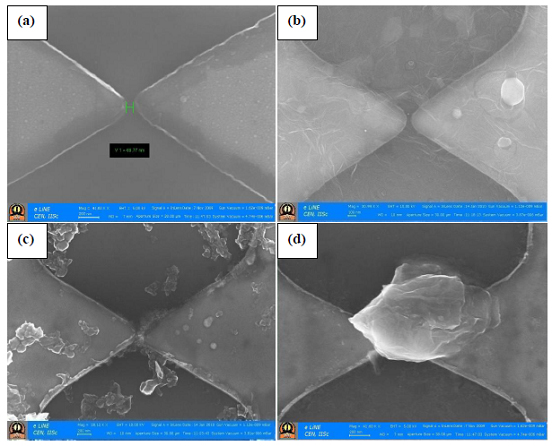 |
| Fig.1: FE-SEM images of two platinum thin-film electrodes separated by 70 nm, (a) without graphene, and (b) with different types of graphene crossing the gap: (b) RGO, (c) HG, and (d) EG |
Abstract:
A timely review analyzing the correlation of synthesis methods and physical properties of single-layer and few-layered graphene flakes.
Graphene: Singles and the few
UK | Posted on November 8th, 2010A review of methods used for synthesizing both single and few-layer graphene and the resulting properties is presented by C.N.R. Rao and colleagues at the Jawaharlal Nehru Centre for Advanced Scientific Research and Indian Institute of Science, Bangalore. The article was published recently in Science and Technology of Advanced Materials.
The group not only compares the electrical, magnetic and surface properties of the resulting graphene [2] but based on their own research, the authors describe the physical properties of graphene-polymer composites and field-effect transistors fabricated using graphene.
Since the first report on the mechanical isolation of graphene from graphite, the interest in the physical properties and potential applications�such as transparent electrodes for solar cells, nano-electronics and robust mechanical structures�has led to an unprecedented increase in the number of publications on the synthesis, properties and applications of this unique 2D-material.
But the field is still in its infancy, with challenges and issues to be resolved, in particular the effects of the synthesis method on the properties of the resulting graphene.
The Nobel Prize in Physics 2010 was awarded to Andre Geim and Konstantin Novoselov of University of Manchester "for groundbreaking experiments regarding the two-dimensional material graphene"�a unique structure of carbon just one atom thick that has caught the imagination of materials scientists world-wide.
The Manchester researchers reported on the extraction and properties of graphene in 2004 [1]. The simplicity of the �synthesis' surprised many scientists, for who would have imagined being able to isolate an atomic layer of carbon from a block of graphite with a piece of adhesive tape?
Single-layer graphene (SLG) is produced by mechanically �peeling off' a layer of carbon from highly ordered pyrolytic graphite, which is then transferred onto a silicon substrate. Chemically, SLG is prepared by the reduction of a dispersion of single-layer graphene oxide with hydrazine. This resulting reduced graphene oxide (RGO) is a black suspension that contains residual oxygen, and this distinguishes it from SLG obtained by other methods.
Non-chemical methods of producing SLG layers include heating Si-terminated (0001) single-crystal 6H-SiC in vacuum between 1250 and 1450 �C for a few minutes and decomposition of hydrocarbons� methane, ethylene, acetylene and benzene� on sheets of catalytic transition metals such as Ni. The authors' own research on chemical vapor deposition on nickel and cobalt films showed the number of layers to depend on the choice of hydrocarbons and experimental conductions, and importantly, that the graphene layers were difficult to remove from the metal surface after cooling.
Well-known methods for producing few-layer graphene are thermal exfoliation of graphite oxide at 1050 �C, the chemical reaction of an aqueous solution of SGO with hydrazine hydrate at the refluxing temperature or by microwave heating, heating 4-6 nm nanodiamond particles in an inert or reducing atmosphere above 1500 �C, and arc evaporation of graphite in a hydrogen atmosphere. The team found the latter method yields graphene with only 2-3 layers of 100-200 nm sized flakes although they note that controlling the number of layers of graphene is still a challenge.
The surface area of graphene is an important parameter for applications such as gas sensing and storage of gases such as hydrogen. In comparison to single-layer graphene, which theory predicts to have a large surface area of 2600 m2/g, measurements by the Bangalore group on few-layer graphene showed the surface area to be 270-1550 m2/g.
The electronic structure of graphene is determined by the �edge states' of graphene flakes, with bilayer graphene predicted to be ferromagnetic. Rao and co-workers showed the Curie-Weiss temperatures obtained from the high-temperature inverse susceptibility data to be negative in all samples measured by them, indicating antiferromagnetism. The authors note the possibility of the coexistence of different types of magnetic states within a single flake of graphene. In addition, all graphene samples showed magnetic hysteresis at room temperature, with electron paramagnetic resonance measurements suggesting that this behavior did not originate from transition-metal impurities.
Electrical measurements showed semiconducting behavior in few-layer graphenes with conductivity increasing between 35 and 300 K, which is different from the metallic nature exhibited by the single-layer graphene, and the electrical conductivity of graphene samples decreased with increasing number of layers. Furthermore, few-layer graphene samples were n-type and suitable for the fabrication of field-effect transistors, and the best transistors were realized with few-layer graphene produced by arc discharge of graphite in hydrogen. In measurements on composites of a polymer and few-layer graphene (PMMA-RGO, PMMA-HG and PVA-EG), the electrical conductivity of the composites increased with increasing graphene content. Thermoelectric measurements revealed a relatively small thermopower in few-layer graphenes compared with single-layer graphene. Interestingly, few-layer graphenes with the largest surface area showed the strongest interaction with electron-donor and acceptor molecules via molecular charge transfer.
This review contains 68 references and 21 figures and provides an invaluable source of up-to-date information for newcomers and experts in this exciting area of research.
References and related websites
[1] Science 306 (2004) p. 666 {www.sciencemag.org/cgi/content/abstract/306/5696/666}
[2] Science and Technology of Advanced Materials 11 (2010) October. {iopscience.iop.org/1468-6996/11/5/054502} Sci Technol Adv Mater Vol.11 (2010) 054502 doi: 10.1088/1468-6996/11/5/054502
[3] Jawaharlal Nehru Centre for Advanced Scientific Research, Bangalore, India {www.jncasr.ac.in/annview.php?id=239}
[4] Solid State and Structural Chemistry Unit, Indian Institute of Science, Bangalore, India
{sscu.iisc.ernet.in/ }
[5] National Institute for Materials Science {www.nims.go.jp/eng/}
####
For more information, please click here
Contacts:
Media contacts:
Mikiko Tanifuji (Ms.)
National Institute for Materials Science, Tsukuba, Japan
Tel. +81-(0)29-859-2494
Copyright © ResearchSEA
If you have a comment, please Contact us.Issuers of news releases, not 7th Wave, Inc. or Nanotechnology Now, are solely responsible for the accuracy of the content.
Bookmark:


| Related News Press |
News and information
![]() Simulating magnetization in a Heisenberg quantum spin chain April 5th, 2024
Simulating magnetization in a Heisenberg quantum spin chain April 5th, 2024
![]() NRL charters Navy�s quantum inertial navigation path to reduce drift April 5th, 2024
NRL charters Navy�s quantum inertial navigation path to reduce drift April 5th, 2024
![]() Discovery points path to flash-like memory for storing qubits: Rice find could hasten development of nonvolatile quantum memory April 5th, 2024
Discovery points path to flash-like memory for storing qubits: Rice find could hasten development of nonvolatile quantum memory April 5th, 2024
Academic/Education
![]() Rice University launches Rice Synthetic Biology Institute to improve lives January 12th, 2024
Rice University launches Rice Synthetic Biology Institute to improve lives January 12th, 2024
![]() Multi-institution, $4.6 million NSF grant to fund nanotechnology training September 9th, 2022
Multi-institution, $4.6 million NSF grant to fund nanotechnology training September 9th, 2022
Chip Technology
![]() Discovery points path to flash-like memory for storing qubits: Rice find could hasten development of nonvolatile quantum memory April 5th, 2024
Discovery points path to flash-like memory for storing qubits: Rice find could hasten development of nonvolatile quantum memory April 5th, 2024
![]() Utilizing palladium for addressing contact issues of buried oxide thin film transistors April 5th, 2024
Utilizing palladium for addressing contact issues of buried oxide thin film transistors April 5th, 2024
![]() HKUST researchers develop new integration technique for efficient coupling of III-V and silicon February 16th, 2024
HKUST researchers develop new integration technique for efficient coupling of III-V and silicon February 16th, 2024
Nanotubes/Buckyballs/Fullerenes/Nanorods/Nanostrings
![]() Tests find no free-standing nanotubes released from tire tread wear September 8th, 2023
Tests find no free-standing nanotubes released from tire tread wear September 8th, 2023
![]() Detection of bacteria and viruses with fluorescent nanotubes July 21st, 2023
Detection of bacteria and viruses with fluorescent nanotubes July 21st, 2023
Nanoelectronics
![]() Interdisciplinary: Rice team tackles the future of semiconductors Multiferroics could be the key to ultralow-energy computing October 6th, 2023
Interdisciplinary: Rice team tackles the future of semiconductors Multiferroics could be the key to ultralow-energy computing October 6th, 2023
![]() Key element for a scalable quantum computer: Physicists from Forschungszentrum J�lich and RWTH Aachen University demonstrate electron transport on a quantum chip September 23rd, 2022
Key element for a scalable quantum computer: Physicists from Forschungszentrum J�lich and RWTH Aachen University demonstrate electron transport on a quantum chip September 23rd, 2022
![]() Reduced power consumption in semiconductor devices September 23rd, 2022
Reduced power consumption in semiconductor devices September 23rd, 2022
![]() Atomic level deposition to extend Moore�s law and beyond July 15th, 2022
Atomic level deposition to extend Moore�s law and beyond July 15th, 2022
Announcements
![]() NRL charters Navy�s quantum inertial navigation path to reduce drift April 5th, 2024
NRL charters Navy�s quantum inertial navigation path to reduce drift April 5th, 2024
![]() Discovery points path to flash-like memory for storing qubits: Rice find could hasten development of nonvolatile quantum memory April 5th, 2024
Discovery points path to flash-like memory for storing qubits: Rice find could hasten development of nonvolatile quantum memory April 5th, 2024
Interviews/Book Reviews/Essays/Reports/Podcasts/Journals/White papers/Posters
![]() Simulating magnetization in a Heisenberg quantum spin chain April 5th, 2024
Simulating magnetization in a Heisenberg quantum spin chain April 5th, 2024
![]() Discovery points path to flash-like memory for storing qubits: Rice find could hasten development of nonvolatile quantum memory April 5th, 2024
Discovery points path to flash-like memory for storing qubits: Rice find could hasten development of nonvolatile quantum memory April 5th, 2024
|
|
||
|
|
||
| The latest news from around the world, FREE | ||
|
|
||
|
|
||
| Premium Products | ||
|
|
||
|
Only the news you want to read!
Learn More |
||
|
|
||
|
Full-service, expert consulting
Learn More |
||
|
|
||